Various sensing elements have become an integral part of modern life. Detector and sensor technologies have improved people’s daily lives through their applications in almost all fields. Different kinds of materials such as silicon, metal oxides, perovskites, transition metal dichalcogenides or carbon-based materials are used to fabricate various detectors and sensors. One of the primary sensor manufacturing requirements for a designer is the fundamental knowledge of bringing new functional material that is sensitive and selective for the monitored events.
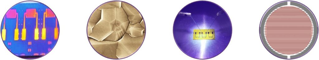
Diamond has gained a reputation as an exceptionally versatile material due to its attractive physical and chemical properties, such as robustness, low dielectric constant, wide bandgap, excellent transparency, high thermal conductivity, and biocompatibility. These fascinating properties make diamond a promising candidate for various applications, i.e. such as cutting and polishing tools, high-power devices, bioelectronic devices or sensors even for harsh environments, etc. Moreover, in combination with other materials in the form of novel heterostructures, the mutual interaction at their interfaces further offers advantageous properties for the fabrication of new devices and sensors that further expand their applicability. In our department, we focus on the design, fabrication and characterization of diamond-based heterostructures and hybrid systems, and the preparation of new sensing devices made from them. As core materials for such heterostructures, we mainly combine diamond with thin layers of transition metal dichalcogenides (TMD), gallium nitride and gallium oxide. To fulfil our ambitious goals, we focus on fundamental material research as well as applied research through testing prepared sensing elements.
1. Fundamental research on diamond heterostructures
Fabrication of diamond heterostructures with TMD is carried out in two different configurations: i) growth of TMD layers on diamond and ii) growth of diamond on TMD layers. Such a combination of opposite and complementary configurations enables a comprehensive investigation of the physical properties of TMD/diamond heterostructures. As an example, Fig. 1a shows an optical image of the boundary area between the nucleated and non-nucleated regions after diamond growth. The nucleated region is overgrown with a continuous nanocrystalline diamond film (SEM image in Fig. 1b). The non-nucleated region reveals a damaged-like surface with locally overgrown carbon-based deposits initiated by spontaneous diamond nucleation. However, Raman measurements (Fig. 1c) confirmed that the MoS2 layer on the non-nucleated region survived the harsh plasma environment during diamond growth.
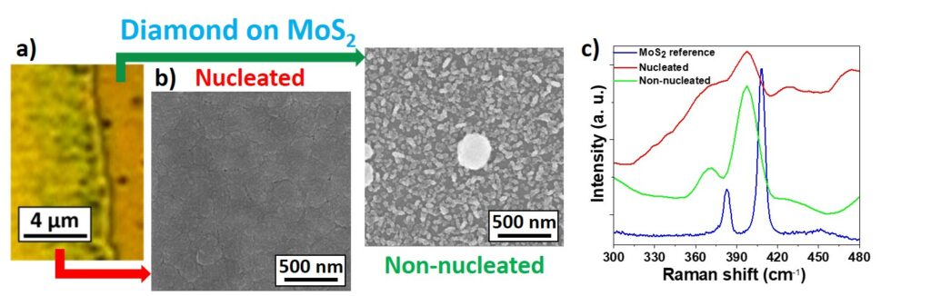
Fig. 1 a) Optical image of the fabricated MoS2/diamond heterostructure highlighted at the boundary of the nucleated and non-nucleated regions of the sample. b) Top-view SEM images and c) Raman spectra of reference and overgrown MoS2 layer.
In addition to various types of TMDs (MoS2, MoSe2, PtSe2, MoTe2, etc.), we also deal with diamond-based heterostructures with metals, GaN, AlGaN, Ga2O3 materials in the form of various sensing and optoelectronic devices. Fig. 2a shows an example of GaN and Ir materials overgrown with a fully-closed polycrystalline diamond film, where a clear interface between the GaN surface and Ir metallization is observed. Another interesting result can be found when we compare the thermally-induced stress in diamond films on samples with and without a SiON interlayer (Fig. 2b). The stress in the thin diamond film grown on the sample with a SiON interlayer is higher by ~0.2 GPa at 50 °C than the induced stress of the sample without SiON, and this Δ stress decreases with increasing temperature.
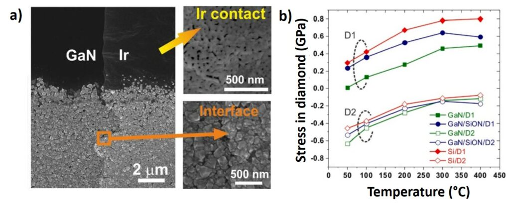
Fig. 2 a) Top-view SEM images of diamond films grown on GaN and Ir with a focus on the interface and b) as measured relative thermally-induced stress in a diamond strip grown on different materials.
2. Applied research – hybrid technologies for diamond detectors and sensors
Radiation sensors and detectors are widely used in fundamental physics, nuclear reactors, aerospace science, medicine, environmental monitoring, etc. In this topic, we focus on the detailed analysis of prepared hybrid detector structures based on mono- and poly-crystalline diamonds. Fig. 3a schematically shows the measuring station and a photograph of one of the prepared samples consisting of a diamond layer on a silicon substrate. Circular metallic contacts with different diameters are prepared on the diamond surface. The manufactured structures are tested using alpha particles with an energy of 4.4 MeV, where the height (voltage) of the measured pulses from individual alpha particles is analysed and the signal-to-noise ratio is also monitored (Fig. 3b). Fig. 3c shows SRIM (Stopping and Range of Ions in Matter) simulation of energy losses of particles in materials.
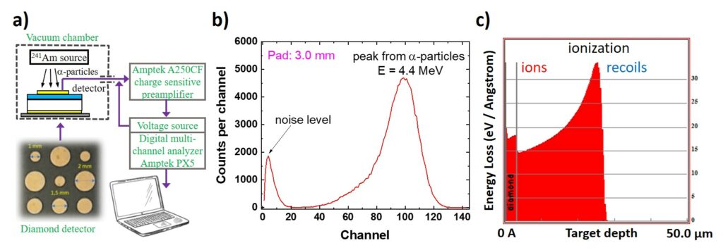
Fig. 3 a) Schematic of the connection of the detector to the spectrometric chain and the distribution of selected upper metallic contacts of different sizes on the diamond layer grown on silicon. b) Spectrum of detected α-particles using a diamond layer with 3 mm contacts. c) SRIM simulation of energy losses of α-particles in a diamond detector.
Gas sensors are essential for industry, healthcare and almost everyday life, with increasing emphasis on detecting hazardous substances and improving air quality. For this reason, the development of sensors based on new materials with high sensitivity, stability and reproducibility for the detection of various gases is in great demand. As part of testing gas sensors, we prepared various sensor structures, including a heterostructure combining polycrystalline diamond and molybdenum disulfide (Fig. 4a, b). From the measured results, this combination of materials appears to be very promising, since the sensor prepared in this way shows increased sensitivity to reducing (NH3) and oxidizing (NO2) gases. The gas interaction model (Fig. 4c) independently considers the influence of each material (chemisorption for MoS2 and surface doping mechanism for hydrogen-terminated diamond) as well as the current flow mechanism through the formed p-n heterojunction. Fig. 4d shows the absolute and relative resistance change of the MoS2/diamond sensor over time depending on the gases used.
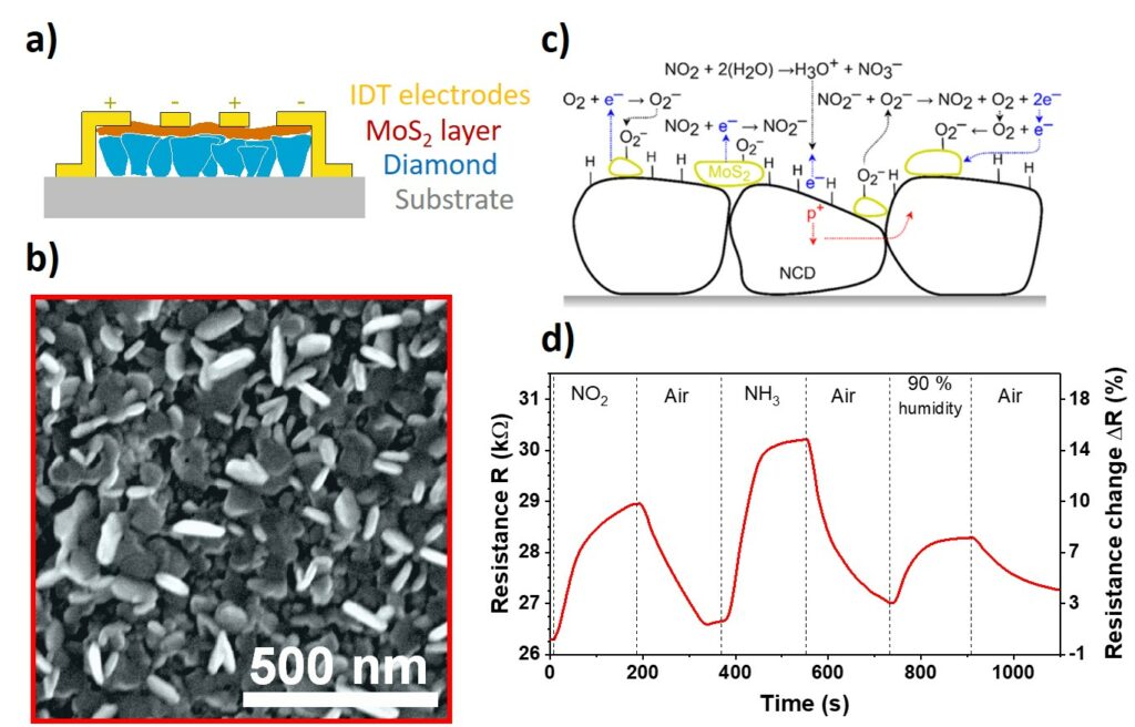
Fig. 4 a) Schematic cross-sectional view and b) corresponding top-view SEM image of the fabricated diamond/MoS2 heterostructure. c) Schematic representation of the gas sensing and charge transport mechanism for two parallel connected layers represented by MoS2 and diamond. d) Time response of the MoS2/diamond sensor to three gases (nitrogen dioxide, ammonia and 90 % humidity).
Research staff:
Selected publications:
Zaťko, M. Varga, G. Vanko, T. Izsak, A. Sagatova, A. Kromka, „Polycrystalline CVD diamond-based structures for detection of charge particles„, Applied Physics of Condensed Matter (APCOM2023) AIP Conf. Proc. 3054, 050013-1–050013-5; https://doi.org/10.1063/5.0187517
Kočí, M., Izsák, T., Vanko, G., Sojková, M., Hrdá, J., Szabó, O., Husák, M., Végsö, K., Varga, M., and Kromka, A.: Improved gas sensing capabilities of MoS2/diamond heterostructures at room temperature, ACS Applied Mater. Interfaces 15 (2023) 34206-34214.
Kočí, M., Szabó, O., Vanko, G., Husák, M., and Kromka, A.: Enhanced gas sensing capabilities of diamond layers using Au nanoparticles, Diamond Related Mater. 138 (2023) 110218.
Varga, M., Sojková, M., Hrdá, J., Parza Saeb, S., Vanko, G., Pribusová-Slušná, L., Ondic, L., Fait, J., Kromka, A., and Hulman, M.: Technological challenges in the fabrication of MoS2/diamond heterostructures. In NANOCON 2022. Proc. 14th Inter. Conf. Nanomater. – Res. & Appl. Ostrava. Tanger Ltd. 2023, pp 21-27. ISBN: 978-80-88365-09-9.
Izsák, T., Vanko, G., Babčenko, O., Zaťko, B., and Kromka, A.: Effects of metal layers on chemical vapor deposition of diamond films, J. Electr. Engn. 73 (2022) 350–354.
Izsák, T., Vanko, G., Babchenko, O., Vincze, A., Vojs, M., Zaťko, B., and Kromka, A.: Influence of SiON interlayer on the diamond/GaN heterostructures studied by Raman and SIMS measurements, Mater. Sci Engn. B 273 (2021) 115434.
Babcenko, T. Izsak, M. Varga, K. Aubrechtova Dragounova, S. Potocky, S. Stehlik, G. Vanko, L. Gajdosova, S. Kasemann, J. Zehetner, A. Kromka, „Optimization of diamond growth on structured, soft and brittle substrates“, In the proceeding „13th International Conference on Advanced Semiconductor Devices and Microsystems, ASDAM 2020, October 11th-14nd 2020, Smolenice, Slovakia, pp. 46-50 (2020)
Izsák, T., Vanko, G., Držík, M., …Potocký, S., Kromka, A.: Front-side diamond deposition on the GaN membranes, ASDAM 2020 – Proceedings: 13th International Conference on Advanced Semiconductor Devices and Microsystems, 2020, pp. 42–45, 9393833