2024
Investigating structural, optical, and electron-transport properties of lithium intercalated few-layer MoS2 films: Unraveling the influence of disorder
Molybdenum disulfide (MoS2) is a frequently studied material due to its layered structure, exceptional properties, and applicability in electronics, optoelectronics, and lithium batteries. In our research, we have shown how the addition of lithium affects the properties of ultrathin MoS2.
The layered structure of MoS2 allows the intercalation of foreign atoms into the van der Waals gaps between the individual layers, which can affect the electronic structure as well as the electrical and optical properties of the material. Our colleagues investigated intercalation of few-layers MoS2 with lithium. The initial few-layers MoS2 were prepared using two different techniques – thermally assisted conversion (TAC) and pulsed laser deposition (PLD). We used a mixture of sulfur and Li2S powders as a source of lithium, which was heated to a high temperature together with MoS2. Through diffusion, lithium entered the space between the MoS2 layers. The presence of lithium in the samples was confirmed using synchrotron radiation photoelectron spectroscopy. We did not observe any structural changes or changes in the optical properties of the layers after intercalation. However, the electrical resistance of the samples with lithium content increased significantly. By measuring the temperature dependence of resistance, we found that carrier transport in our layers is best described by Efros-Shklovskii variable range hopping, typical for a disordered semiconductor. Since the resistance of the layers increased significantly with increasing lithium content, we can conclude that lithium introduced new disorder into our layers, resulting in increased resistance. Even if lithium donated electrons to the MoS2 layers, this effect remained hidden due to the prevailing disorder effect.
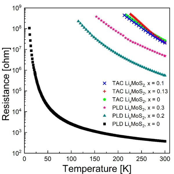
The electrical resistance dependence on temperature, x in LixMoS2, refers to Li content in MoS2 layers.
Outputs:
Hrdá, J., Moško, M., Píš, I., Vojteková, T., Pribusová Slušná, L., Hutár, P., Precner, M., Dobročka, E., Španková, M., Hulman, M., Chromik, Š., Šiffalovič, P., Bondino, F., and Sojková, M.: Investigating structural, optical, and electron-transport properties of lithium intercalated few-layer MoS2 films: Unraveling the influence of disorder, Applied Phys. Lett. 124 (2024) 123101.
2023
Lithium-induced reorientation of few-layer MoS2 films
In our research, we focused on studying the influence of lithium on the growth of ultrathin layers of molybdenum disulfide (MoS2). The positive impact of lithium has already been demonstrated in the enhanced catalytic performance of lithium-doped MoS2 layers in hydrogen production and CO2 reduction. Lithium doping also has the potential to improve lithium battery technology.
MoS2 is a layered material that can be prepared in the form of single or few-layer films. Due to its interesting properties and wide range of potential applications, this material is the subject of extensive study. Intercalation is one way to influence the physical, chemical, and electronic properties of materials. However, the effect of lithium on the growth of MoS2 layers has not been fully explored.
In our work, we used a novel approach to incorporate lithium into MoS2 layers. MoS2 fabrication involved one-zone sulfurization of pre-deposited molybdenum layers. Lithium sulfide was used as the source of lithium. Structural analyses show a remarkable effect of lithium, supporting epitaxial and horizontal layer growth. After annealing in the presence of Li, MoS2 layers tend to grow horizontally even for thicker initial molybdenum layers. The most surprising observation is the conversion of vertical MoS2 layers to horizontal after annealing in the presence of Li. We hypothesize that lithium acts as a catalyst facilitating this conversion.
Our work demonstrates that lithium doping can alter the orientation of the basal plane of MoS2 in very thin layers. As already shown, vertically and horizontally oriented layers exhibit different electronic, chemical, and optical properties. Therefore, control over the crystallographic orientation of MoS2 will be crucial in designing next-generation devices containing MoS2 layers.
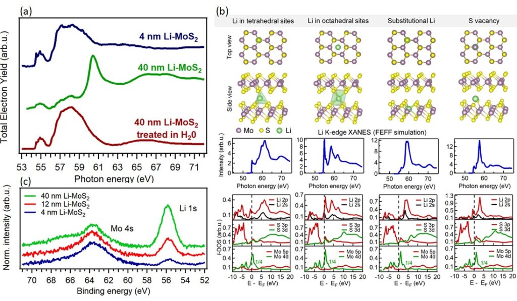
(a) Li K-edge XANES spectra for Li doped 2H-MoS2 measured at the beamline BACH (b) Li K-edge XANES spectra obtained by FEFF calculations. Top: fragments of the structural models for hexagonal 2H-MoS2 with atoms in tetrahedral and octahedral interstitial sites, substitutionally doped MoS2, and with lithium near a single sulfur vacancy. Middle: simulated Li K-edge XANES spectra. Bottom: calculated orbital-projected density of states for Li, S, and Mo atoms.(c) Mo 4s and Li 1s XPS spectra from Li doped MoS2 samples.
Outputs:
Sojková, M., Píš, I., Hrdá, J., Vojteková, T., Pribusová Slušná, L., Vegso, K., Šiffalovič, P., Nádaždy, P., Dobročka, E., Krbal, M., Fons, P.J., Munnik, F., Magnano, E., Hulman, M., and Bondino, F.: Lithium-induced reorientation of few-layer MoS2 films, Chem. Mater. 35 (2023) 6246-6257.
2022
Analysis of inhomogeneous Au/Ni/4H-SiC Schottky diodes and intersection of their temperature dependent I-V curves
In connection with preparation of surface barrier detectors radiation detectors from 4H-SiC we studied temperature dependence of electrical parameters of Schottky barrier of Au/Ni/4H-SiC diode in the temperature range 35 – 80 °C [1]. I-V curves (Fig. 1) have not a linear part in semi-logarithmic plot which could be a result of an inhomogeneity in the barrier height. Therefore we analysed I-V curves at the assumption of Gaussian barrier height distribution of parallely connected diode patches with their own series resistance. By the least squares method we determined the mean barrier height of the barrier distribution, the standard deviation and the series resistance as a function of temperature (Fig. 2).
The extracted mean barrier height as well as the standard deviation decreased with increasing temperature. On the other hand the series resistance inreased with increasing temperature. The consequence of increasing the series resistance was an intersection of the I-V curves in common point (approximately common), which was practically independent (very slightly dependent) on temperature.
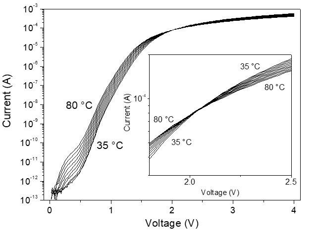
Fig. 1
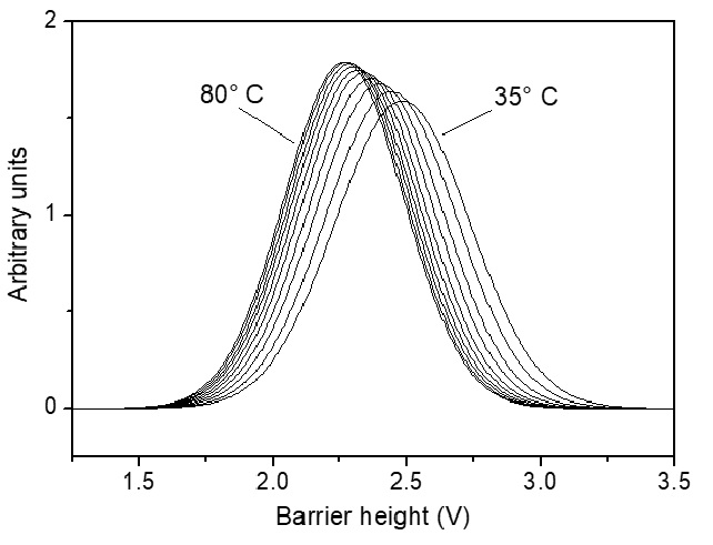
Fig. 2
We analyzed further whether there is only one intersection point or there is a voltage interval where the I-V curves intersect [2]. We studied three cases – homogeneous diode, inhomogeneous diode which can be treated as a set of small diodes where each one of them has its own series resistance and inhomogeneous diode with one common series resistance. For the studied temperature region 300 – 400 K we obtained by numerical methods for the diodes with certain parameters that the smallest dispersion between the the voltage (current) of intersection points has homogeneous diode, higher dispersion was obtained for inhomogeneous diode with the common series resistance and the highest dispersion for the diode which is a parallel connection of small diodes with their own series resistance.
Outputs:
[1] J. Osvald, L. Hrubčín, B. Zaťko, Temperature dependence of electrical behaviour of inhomogeneous Ni/Au/4H–SiC Schottky diodes, Mat. Sci. Semicond. Process. 140 (2022) 106413.
[2] J. Osvald, Intersection of 4H-SiC Schottky diodes I–V curves due to temperature dependent series resistance, Semicond. Sci. Technol. 37 (2022) 125003.
2021
Fabrication and study of few-layer PtSe2 films
Few-layer PtSe2 films are promising candidates for applications in high-speed electronics, spintronics and photodetectors. We reported the fabrication of epitaxially aligned PtSe2 films using one-zone selenization of pre-sputtered platinum layers on the c-plane sapphire substrate. The use of elevated temperature led to enhanced crystallinity and better electrical properties.1 Moreover, we have identified the Se : Pt ratio as a parameter controlling the charge carrier mobility in the films. The mobility increases more than twice as the ratio changes in a narrow interval around a value of 2.2 Combining a semiconductor with a superconductor on a single platform is expected to provide devices with improved performance. we report on the fabrication of a few-layer PtSe2 film on top of an NbN substrate. We found the selenization parameters preserving the chemical and structural integrity of both the PtSe2 and NbN films. The PtSe2 film alignment can be tuned by varying the nitrogen flow rate through the reaction chamber.3
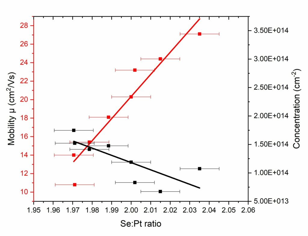
Fig. 1 Se : Pt ratio vs. charge carrier mobility and carrier concentration of PtSe2 films prepared by selenization of 1 nm thick Pt layer at 550 °C during 30 min with different N2 flow rate
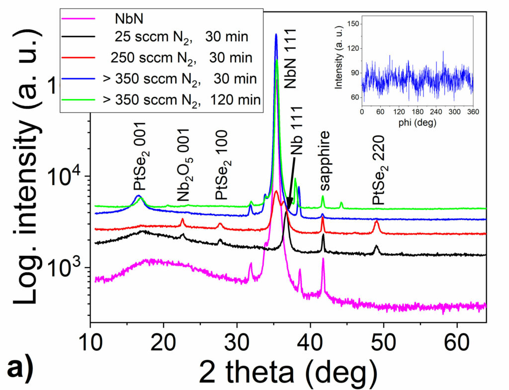
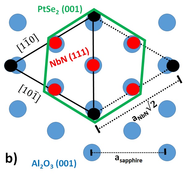
Fig. 2. (a) XRD pattern of NbN substrate layer and PtSe2 films prepared by selenization of 3 nm thick platinum layer at 550 °C on the NbN substrate using different nitrogen flow rates and annealing times. (b) Schematic sketch showing the arrangement of a PtSe2 films on an NbN / sapphire substrate.
Outputs:
1, Sojková, M., Dobročka, E., Hutár, P., Tašková, V., Pribusová Slušná, L., Stoklas, R., Píš, I., Bondino, F., Munnik, F., and Hulman, M.: High carrier mobility epitaxially aligned PtSe2 films grown by one-zone selenization, Applied Surface Sci 538 (2021) 147936.
2. Hrdá, J., Tašková, V., Vojteková, T., Pribusová Slušná, L., Dobročka, E., Píš, I., Bondino, F., Hulman, M., and Sojková, M.: Tuning the charge carrier mobility in few-layer PtSe2 films by Se: Pt ratio, RSC Adv. 11 (2021) 27292. (APVV 17-0352, 17-0560, 19-0365, VEGA 2/0059/21, CEMEA ITMS 313021T081)
3. Sojková, M., Hrdá, J., Volkov, S., Vegso, K., Shaji, A., Vojteková, T., Pribusová Slušná, L., Gál, N., Dobročka, E., Šiffalovič, P., Roch, T., Gregor, M., and Hulman, M.: Growth of PtSe2 few-layer films on NbN superconducting substrate, Applied Phys. Lett. 119 (2021) 013101.
2020
Schottky barrier height inhomogeneity in 4H-SiC surface barrier detectors
We investigate the Schottky barrier height of Au/Ni/4H-SiC structures designated for detection of ionizing radiation. The current-voltage and capacitance-voltage measurements were utilized for analyzing of three diode parameters – barriere height, ideality factor and series resistance. We found out that the barrier height is not possible to analyse with only one barriere height of the whole area of a diode. Following we used the analyzis of Gauss barrier height distribution. The experimental current-voltage curves we simulataed with two diffirent influences of seriers resistance on structures using two algorithms. In the first case we assumed that the Schottky diode is created from a lot of parallel non-interacting smaller diodes and each has a different series resistance. In the second case we also assumed a lot of parallel Schottky diodes but with one common series resitance. In both approaches we searched three parameters – mean value of the barrier Gauss distribution, mean square deviation of the distribution and series resistance of diode.
Results shows that current-voltage measurements are good fitted with the first approach while the second has much higher variance with real measurements.
Outputs:
Osvald, J., Hrubčín, L., and Zaťko, B.: Schottky barrier height inhomogeneity in 4H-SiC surface barrier detectors, Applied Surface Sci 533 (2020) 147389.
2019
2018
2017
- Thermo-mechanical analysis of uncooled La0.67Sr0.33MnO3 microbolometer made on circular SOI membrane
2016
2015
- Terahertz radiation detector
- Nanomachining with subsequent polishing of the active surfaces of crystal X-ray optics
2014
- Semiconductor pressure sensor for extreme conditions
- Spectrometric detector of heavy ions based on 4H-SiC
2013
- Phase contrast X-ray imaging of light weight samples
- The way of patterning of Tl-based superconducting thin films