 Contact
 Intranet
 SK
SK


MOCVD laboratory
Contact info: doc. Ing. Novák Jozef, DrSc.
The MOCVD laboratory (established in July 1993) runs two epitaxial equipments from Aixtron provenience. The older equipment, AIXTRON AIX-200 R&D, is a standard research-oriented apparatus allowing growth of III-V semiconductor epitaxial layers and advanced heterostructures on GaAs, GaP, and InP substrates. Elements of group III are supplied from basic organometallic sources, such as trimethylgallium (TMGa), trimethylindium (TMIn), trimethylaluminum (TMAl), and group V elements are incorporated from hydrides, such as arsine (AsH3) and phosphine (PH3). Doping sources used are diethylzinc (DEZn) for Zn and silane for Si. MOCVD equipment is used for the preparation of epitaxial layers, heterostructures, and low dimensional structures in InxGa1-xP/GaAs, AlGaAs/GaAs, InxGa1-xAs/GaAs, and InxGa1-xAs/InP material systems.
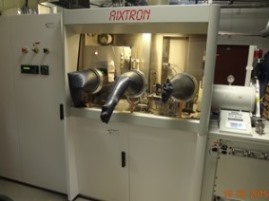
Since December 2014 we operate a new Aixtron CCS flip top MOCVD system with shower head-type of reactor. It allows growth on 3×2 or 1×4-inch wafers. This equipment is dedicated for growth of GaN based epitaxial layers and structures. Recently TMGa, TEGa, TMAl, and TMIn sources are incorporated as group III element sources. NH3 serves as a nitrogen source while the silane is used for Si doping. The sources arrangement allows growth of GaN, InAlN, AlGaN, and InGaN layers and structures. Our goal is to optimise growth processes aiming the preparation of layers and heterostructures with high quality crystallographic structure interface quality on the atomic level for application in advanced transistor and photocathode structures.
Scope:
- MOVPE growth nitrides, arsenides, and phosphides
- Growth of doped and undoped nanowires including an analysis of early stages of nanowire growth
- Preparation of photonic structures based on NSOM lithography patterning
Equipment:
- MOVPE Aixtron CCS 3×2 shower head reactor for GaN and related compounds
- MOVPE horizontal equipment Aixtron AIX-200 for growth of arsenides and phosphides

contact for more info: Ing. S. Hasenöhrl, Ing. J. Kuzmík, DrSc.
Optical laboratory
Contact info: RNDr. Kučera Michal, PhD.
The laboratory is used to perform optical characterization of semiconductor materials and structures. Standard spectroscopic techniques can be applied at room as well as cryogenic temperatures. Rich information on material electronic properties can be deduced from the spectra, including band-gap width, optical transitions in QWs, crystalline quality, impurity identification.
Scope
- Photoluminescence is the most important tool for optical investigation of the electronic structure of semiconductors.
- Photoreflectance is used to evaluate semiconductor band-gap and transition energies in QWs with a good precision even at room temperature.
- Photoconductivity represents a precise and simple tool to investigate some absorption processes in materials.
- Transmittance yields useful information especially about properties of band-edge regions of semiconductor energy spectra.
- Responsivity gives spectral dependences of photo-responses of experimental semiconductor structures, and it indicates their overall performance.
Equipment
- Sample cooling: optical cryostat with a precise temperature regulation in the 4-300 K range.
- Pumping lasers: Helium-Neon (633 nm, 10 mW), Argon-ion (488 nm, 20 mW).
- Broadband light source: THL lamp 150 W, spectral range 300-2500 nm.
- Monochromators: Digikrom 240 (CVI Laser Corp., f 240 mm, 500-2800 nm range), MSH-300 (LOT-QuantumDesign GmbH, f 300 mm, 200-2400 nm range), SR500 (Andor Technology Ltd., f 500 mm, 200-2500 range).
- Detectors: PMT (TE-cooled, 200-850 nm), Si photodiode (400-1100 nm), Ge photodiode, RT (800-1800 nm) or LN2-cooled (700-1500 nm), InGaAs photodiode LN2-cooled (extended wavelength range 700-2600 nm at RT, 700-2250 nm with LN2), PbS photoconductor LN2-cooled (1-4 µm).
- Lock-in amplifiers: model 5210, EG&G Princeton Applied Research Corp.
