2021
- InN: breaking the limits of solid-state electronics
InN has been predicted to be among the top candidates for materials with the highest electron velocity. However, this theoretical prediction has not been validated yet. In the present work, we demonstrate state-of-the art InN material with an electron drift velocity of about 1 × 10⁸ cms-1 at an electric field of 48 kVcm-1. This is the highest steady-state electron velocity ever measured in any solid-state device. Even more, our experimental value outperforms theoretical predictions by a factor of two suggesting a need for revised understanding of InN fundamental properties. If technology of InN-channel transistors is fully developed, present THz frequency gap between the electronic and optical devices will be erased.
This work has been performed in collaboration with University of Crete and MRG IESL Crete.
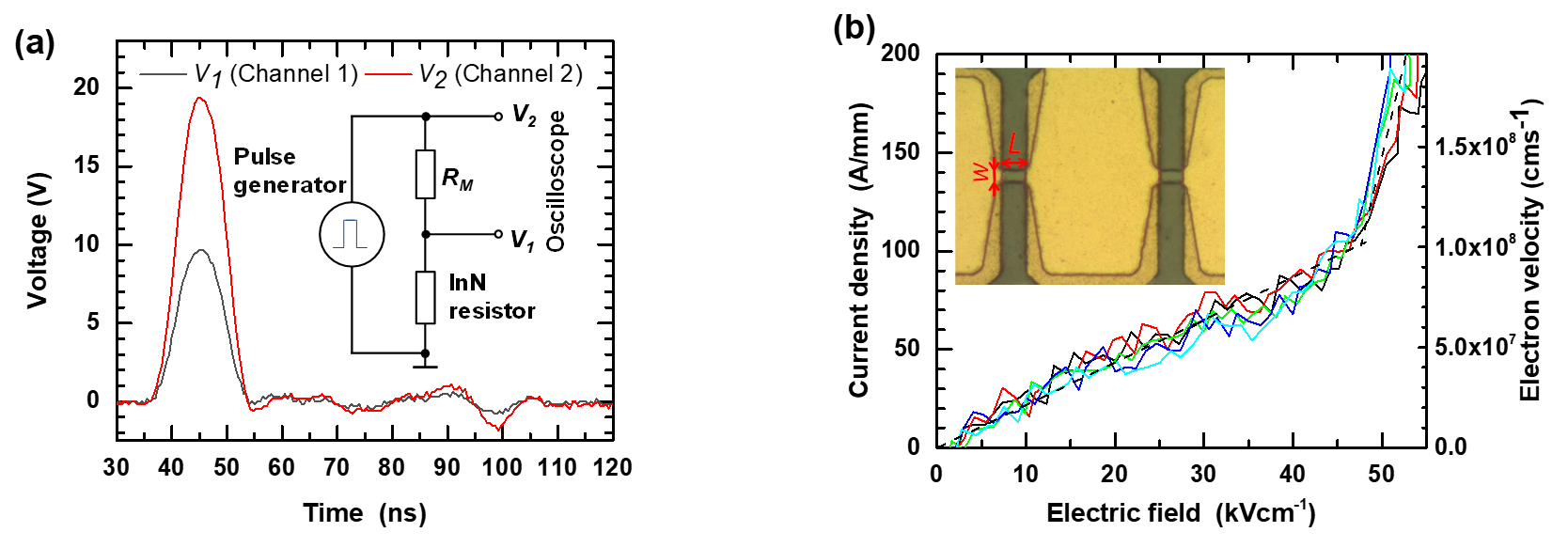
Current-voltage characterization and electron velocity extraction of InN resistors. (a) Typical 10-ns long current-voltage waveform. Rise and falling time was about 6 ns. To construct current-voltage characteristics shown in (b), waveforms were averaged over 2-ns time span around the peak. Sketch of the measurements set-up is depicted in the inset. HP 8114A 100 V/2 A was used as a programmable pulse generator, Rm = 8.5 W. (b) Current density dependence on the applied electric field (left-side axis) and corresponding extracted electron drift velocity (right-side axis) on a series of resistors. Dash lines interpolate the values. Inset shows optical microscope view of two 8-mm long and 4-mm wide InN test resistors. Non-alloyed Ti/Al/Ni/Au ohmic contacts and bottom GaN surface exposed by dry etching are clearly distinguishable.
J. Kuzmík, A. Adikimenakis, M. Ťapajna, D. Gregušová, Š. Haščík, E. Dobročka, K. Tsagaraki, R. Stoklas, A. Georgakilas: InN: breaking the limits of solid-state electronics, AIP Advances 11 (2021) 125325.
2020
- Growth and Properties of N-polar InN/InAlN Heterostructures
InN has been reported as a promising material for ultra-high frequency transistors. This was particularly because of theoretically predicted record electron drift velocity, highest from all common semiconductors. However, no microwave InN-channel transistor has been demonstrated till now. It can be suggested that the In-rich InAlN buffer layer can reduce density of dislocations in InN by providing lower lattice mismatch if compared with more common growth on GaN. Consequently, in N-polar InN/InAlN heterostructure we could demonstrate decent electron mobility of 720 cm2V-1s-1 with InN layer as thin as 20 nm. Because of improved InN crystalline quality, Hall data of the N-polar InN/InAlN heterostructure grown on on-axis sapphire was superior to the ones on off-axis sapphire. Further improvement of the mobility beyond the present state-of-the art can be obtained by InAlN surface smoothing, In molar fraction increase and by compensating InAlN unintentional doping. In our work we show viable steps towards InN-channel HEMTs.

a) XRD 2θ/ω diffraction curve of InN(20 nm)/In0.57Al0.43N heterostructure grown on on-axis sapphire, b) 2D and 3D views of 2×2 µm2 AFM scans of 20 nm thick InN grown on N-polar In0.57Al0.43N layer, c) InN electron mobility and concentration dependence on InN thickness.
Hasenöhrl, S., Dobročka, E., Stoklas, R., Gucmann, F., Rosová, A., and Kuzmík, J.: Growth and Properties of N-polar InN/InAlN Heterostructures, Phys. Stat. sol (a) 217 (2020) 2000197.
Kučera, M., Hasenöhrl, S., Dobročka, E., Rosová, A., Eliáš, P., Gucmann, F., and Kuzmík, J.: Morphology, crystalline quality, and optical properties of MOCVDgrown InN/InAlN heterostructures. In: ASDAM 2020. Eds. T. Izsák et al. IEEE 2020. ISBN 978-1-7281-9776-0. P. 131-134.
2019
- Growth of In-rich InAlN by MOCVD
We correlated In-incorporation with residual strain/relaxation in InAlN layers. In-rich InAlN is needed as a buffer for InN channel transistors. Growths directly on sapphire or on GaN/sapphire template were tested. In comparison to later one, full relaxation in InAlN grown on sapphire was observed. Consequently, an increase of the In-molar fraction from 0.28 to 0.60, if compared with the GaN template was obtained.

a) Representative XRD 2θ/ω scan of In0.60Al0.40N grown on (0001) sapphire, b) Negative Cs HRTEM image of InxAl1-xN layer of sample grown on sapphire showing aligned columns of N atoms (blue) and In/Al atoms (red), c) In, N, Al, O and C elemental depth profiles in InxAl1-xN layers along the growth direction [0001].
Chauhan, P., Hasenöhrl, S., Dobročka, E., Chauvat, M.-P., Minj, A., Gucmann, F., Vančo, Ľ., Kováč, J.jr., Kret, S., Ruterana, P., Kuball, M., Šiffalovič, P., and Kuzmík, J.: Evidence of relationship between strain and In-incorporation: growth of N-polar In-rich InAlN buffer layer by OMCVD, J. Applied Phys. 125 (2019).
Chauhan, P., Hasenöhrl, S., Minj, A., Chauvat, M.P., Ruterana, P., and Kuzmík, J, Growth evolution of N-polar Indium-rich InAlN layer on c-sapphire via strain relaxation by ultrathin AlON interlayer, Applied Surface Sci 502 (2020) 144086.
Chauhan, P., Hasenöhrl, S., Dobročka, E., Vančo Ľ., Stoklas, R., Kováč, J., Šiffalovič, P., and Kuzmík, J.: Effect of temperature and carrier gas on the properties of thick InxAl1-xN layer, Applied Surface Sci 470 (2019) 1-7.
Hasenöhrl, S., Chauhan, P., Dobročka, E., Stoklas, R., Vančo, Ľ., Veselý, M., Bouazzaoui, F., Chauvat, M.-P., Reterana, P., and Kuzmík, J.: Generation of hole gas in non-inverted InAl(Ga)N/GaN heterostructures, Applied Phys. Express 12 (2019) 014001.
2018
- Study of surface charges in III-N heterostructures for preparation of GaN power switching devices
In last two decades, III-N high-electron mobility transistors (HEMTs) have gained a large interest due to outstanding prospect for high frequency and power applications. This was also due to a specific phenomenon of polarization doping, when a large-density two-dimensional electron gas (2DEG) is formed in the quantum well (QW) at a III-N barrier/channel interface by compensating the residing polarization charge. This mechanism is completely different from more conventional modulation doping in e.g. GaAs-based HEMTs, when 2DEG formation is driven by a barrier/channel conduction band discontinuity (DEC) and the barrier impurity doping. For polarization doped III-N MOST HEMTs we suggest that i) ionized surface donors behave like a fixed charge and are distinguishable from trapping states, ii) open channel drain current is independent on the surface donor density, iii) if Nd,surf > PQW/q than 2DEG is populated by electrons transferred from surface donors, and iv) if Nd,surf < PQW/q than at channel opening 2DEG is populated both by surface donors (if not completely eliminated) and injecting source contact.

Dependence of (a) maximum drain current (IDSmax) and (b) threshold voltage (Vth) on the oxide thickness (tox) of Ni/Al2O3/AlGaN/GaN MOS heterostructures with and without post-deposition annealing (PDA) of Al2O3 gate dielectric grown by MOCVD. The slope of the latter is used for the surface donor density determination (Nd,s). (c) and (d) shows C-V characteristics and extracted maximum 2DEG density (n2DEG) for structures corresponding to those shown in (a) and (b).
Gucmann, M. Ťapajna, O. Pohorelec, Š. Haščík, K. Hušeková, and J. Kuzmík: Creation of two-dimesional electron gas and role of surface donors in III-N metal-oxide-semiconductor high-electron mobility transistors. Phys. Status Solidi A 215 (2018) 1800090.
Ťapajna, M., Drobny, J., Gucmann, F., Hušeková, K., Hashizume, T., and Kuzmík, J.: Impact of oxide/barrier fixed charge on threshold voltage instabilities in AlGaN/GaN metal-oxide-semiconductor heterostructures. In: Inter. Workshop on Nitride Semicond. (IWN 2018) Kanazawa 2018.
2017
- Vertical GaN transistor with insulating channel and the method of preparation
Securing an ecological development of the society is closely linked with new ways of effective exploitation of available energy sources. One possibility is to minimize losses in electrical converters. To maximize the power in the same time, usage of the GaN-based power transistors is extremely useful.GaN is chemically stable semiconductor material with an energetic band-gap of 3.4 eV, which predestine its usage in hostile environment and at elevated temperature above 300 °C. Apart from that, high electron drift velocity of about 1 x 10⁵ m/s provides GaN transistors with possibility to switch at high frequency. These material parameters are extremely useful for a construction of high power and frequency transistors and converters with high efficiency.
Basis of the invention is a vertical GaN transistor, consisting of an emitter electrode on the top contacting n+ GaN layer, collector electrode placed on a bottom of a GaN substrate and a gate electrode. Gate electrode is formed vertically along the insulating GaN channel and is separated from the GaN semiconductor by a dielectric insulator layer having a larger band-gap as for GaN. Insulating nature of the GaN channel provides for transistors an enhancement mode of operation, along with massive device construction without necessity of nano-patterning, parallel combination of channels, or air-bridge connections for the emitter.
High power vertical GaN transistors with insulating GaN channel will find exploitation by constructing highly effective electric converters. They will be used by energy generation and distribution, as well as in electric cars.
Patent application no. PP50074-2017
2016
- Investigation of gate-diode reliability in switching GaN transistors for high-efficiency converters
Application of GaN-based switching devices (transistors) can lead to suppression of conversion losses in AC/DC and DC/DC converters, when compared to state-of-the-art Si counterparts. This could potentially lead to energy savings with the scale 10-times exceeding supply of renewable generation. Consortia of 7FP EU project HipoSwitch, in which we took a part, aimed the development of full added-value chain based in EU for this new technology. One of the issues identified during the project implementation was the gate-electrode reliability of the GaN transistor operating in ON state. In cooperation with Ferdinand-Braun Institute Berlin (Germany), we investigated the gate degradation upon electrical stress in such conditions. Using the appropriate statistic techniques, we extrapolated the safe operation area for the gate voltage guaranteeing 10-years-lifetime. The results were published in the international conference and renowned scientific journals Applied Physics Letters and IEEE Electron Device Letters.
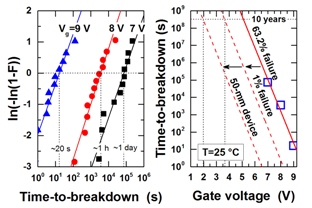
Ťapajna, M., Hilt, O., Bahat-Treidel, E., Würfl, J., and Kuzmík, J.: Gate reliability investigation in normally-off p-type-gan cap/AlGaN/GaN HEMTs under forward bias stress, IEEE Electron Device Lett. 37 (2016) 385 – 388.
Ťapajna, M., Hilt, O., Bahat-Triedel, E., Würfl, H., and Kuzmík, J.: Investigation of gate-diode degradation in normally-off p-GaN/AlGaN/GaN high-electron-mobility transistors, Applied Phys. Lett. 107 (2015) 193506.
Ťapajna, M., Hilt, O., Bahat-Treidel, E., Würfl, J., and Kuzmík, J.: Gate robustness analysis of normally-off p-GaN HEMTs for high power switching applications, In: Proc. 39th Workshop on Compound Semiconductor Devices and Integrated Circuits, WOCSDICE 2015. P. 67-68.
2015
- Material properties of InN layer surfaces
InN is material with the highest saturated velocity of electrons from all existing semiconductors. Consequently, InN is a candidate for designing extremely fast transistors. However, till now there is no report on InN-based microwave transistors. This is because of high strain from the back-side if InN is grown on GaN and because of electron accumulation on the InN surface. In our work we analyzed electrical and chemical properties of InN layers grown with different polarity and methods of removing electrons surface accumulation. Significant oxidation at the In-polar InN surface was found by analyzing photo-electrons emitted from atoms core shells. Similarly, we observed significant surface electron accumulation regardless of the oxide presence. On the other hand, if the InN was capped by four mono-layer of GaN, surface accumulation was fully removed. This effect is vital for manufacturing future ultra-fast InN transistors.
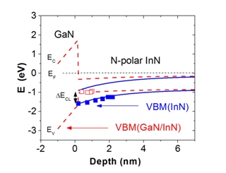
Calculated energy band diagram of N-polar InN (000-1) film without capping (solid line) and with 4 mono-layers GaN cap (dashed line). Experimental values are highlighted by arrows and symbols.
Kuzmik, J., Haščík, Š., Kučera, M., Kúdela, R., Dobročka, E., Adikimenakis, A., Mičušík, M., Gregor, M., Pleceník, A., and Georgakilas, A.: Elimination of surface band bending on N-polar InN with thin GaN capping, Applied Phys. Lett. 107 (2015) 191605.
Kuzmík, J., Adikimenakis, A., Gregor, M., Mičušík, M., Eičo, K., Haščík, Š., Plecenik, A., and Georgakilas, A.: Impact of polarity and GaN capping on electrical and material properties of InN surfaces. In: 11th Inter. Conf. on Nitride Semicond. Peking, 2015.
2014
- Technology transfer of normally-off AlGaN/GaN HEMTs to Ferdinand Braun Institute Berlin
Technology transfer to the Ferdinand Braun Institute Berlin was contracted within the 7FP project HipoSwitch. As a part of European consortia, research group led by Dr. Kuzmik at the Institute of Electrical Engineering Slovak Academy of Sciences, developed a new type of AlGaN/GaN transistors. These devices are envisaged in e.g. high-power and effective converters of electric and hybrid cars. It was necessary to propose a technology which could guarantee sufficiently high values of the transistor switching threshold voltage, as well as sufficiently low on-state resistance, and analyze mechanisms of electrical breakdown in off-state. Our proposed technology of manipulating the transistor threshold voltage is based on semiconductor surface plasma oxidation and subsequent oxide deposition in atomic layers. Using this method we have reached the threshold voltage as high as 1.6 V simultaneously with a current density 0.5 A/mm. Analysis of the off-state breakdown pointed on avalanche mechanism coupled with degrading of interfaces. Apart from scientific papers, our results were represented by industrial samples delivered to our partners.
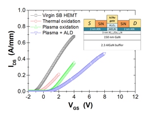
Transfer characteristics of the virgin Schottky-barrier and alternatively oxidized (Al2O3)/AlOxN/AlGaN/GaN HFETs. Inset shows schematic picture of the GaN HFET with a polarization doped access region, plasma oxidized gate region and ALD grown Al2O3.
Gregušová, D., Jurkovič, M., Haščík, Š., Blaho, M., Seifertová, A., Fedor, J., Ťapajna, M., Fröhlich, K., Vogrinčič, J., Liday, J., Derluyn, J., Germain, M., and Kuzmík, J.: Adjustment of threshold voltage in AlN/AlGaN/GaN high-electron mobility transistors by plasma oxidation and Al2O3 atomic layer deposition overgrowth, Applied Phys. Lett. 104 (2014) 013506.
Kuzmík, J., Jurkovič, M., Gregušová, D., Ťapajna, M., Brunner, F., Cho, E.M., Menghesso, G., and Wuerfl, J.: Degradation of AlGaN/GaN high-electron mobility transistors in the current-controlled off-state breakdown, J. Applied Phys. 115 (2014) 164504.
- Design optimization of high-power AlGaN/GaN HEMT switches
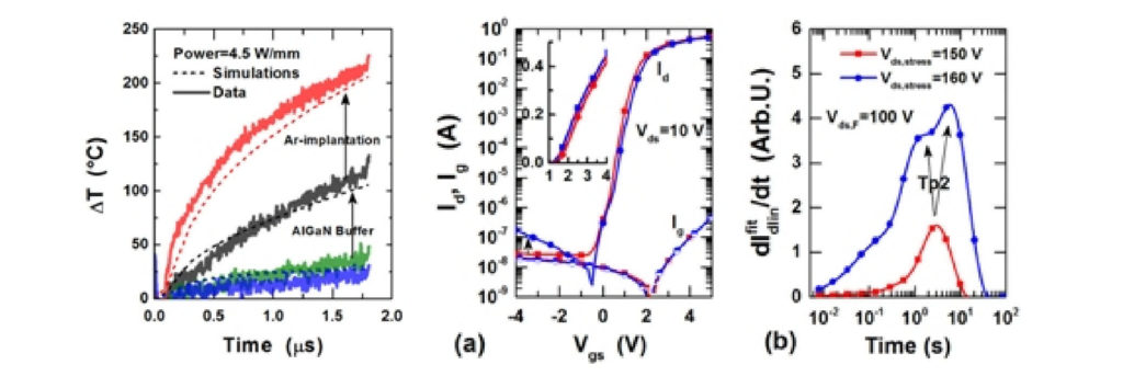
We have investigated self-heating effects and trapping characteristics in tailored normally-off p-GaN/AlGaN/GaN HEMTs. To improve the high-voltage performance, devices were grown with AlGaN or Fe-doped GaN buffer with or without Ar implantation into conductive SiC substrate prior to heterostructure growth. Our transient self-heating analysis indicated almost three-fold higher temperature rise in the transistors with AlGaN buffer compared to devices employing GaN buffer. Surprisingly, the transient self-heating was further increased in devices with AlGaN buffer with Ar implantation into SiC substrate. This effect could be explained by different material parameters of the AlGaN buffer grown on Ar implanted substrate. Modelling indicated AlGaN thermal conductivity to drop from 30 to 15 W/mK for samples without and with Ar implanted into SiC.
To understand the effect of Ar implantation into SiC in more detail, trapping processes were characterized using drain current transient analysis. It revealed appearance of a dominant trapping process (labelled as Tp2 in figure below) in the devices with AlGaN buffer, while being negligible in those with GaN buffer. To localize the trapping centers, drain current transients were measured on devices subjected to step-stress experiment in the off-state. The investigation suggested that dominant trapping centers (Tp2) are located in the AlGaN buffer. This indicates that Ar implantation into SiC substrate influences the density of in-grown defects in the buffer.
Kuzmík, J., Ťapajna, M., Válik, L., Molnár, M., Donoval, D., Fleury, C., Pogany, D., Strasser, G., Hilt, O., Brunner, F., and Wuerfl, J.: Self-heating in GaN transistors designed for high-power operation, IEEE Trans. Electron Dev. 61 (2014) 3429-3434.
M. Ťapajna, et al. In: ASDAM ’14. Eds. J. Breza et al. Piscataway: IEEE 2014. ISBN: 978-1-4799-5474-2, p. 121.
- InGaAs/GaAs metal-oxide-semiconductor heterostructure field-effect transistors with native oxide and Al2O3 double-layer insulator
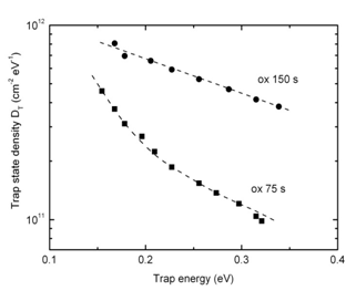
In this study preparation and properties of InGaAs/GaAs MOS structures with double-layer insulator consisting of oxygen-plasma oxide covered by Al2O3 are presented. Structures with 75 s and 150 s oxidation time were used. Static measurements yielded saturation drain current of ~250 mA/mm at VG = 1 V. Capacitance measurements showed improved performance in depletion region comparing with structures without double-layer insulator. Trapping effects were investigated by conductance vs frequency measurements. Trap state density in order of 1011 cm-2eV-1 with its continuous decrease with increased trap energy was evaluated. Carrier mobility evaluation showed peak values of 3950 cm2V-1s-1s for 75 s and 4570 cm2V-1s-1s for 150 s oxidation times with the sheet charge density ~2 × 1012 cm-2. All these demonstrate high capability of used preparation procedure of GaAs-based MOS devices with oxidized GaAs surface covered by Al2O3 insulator.
Gucmann, F., Gregušová, D., Stoklas, R., Dérer, J., Kúdela, R., Fröhlich, K., and Kordoš, P.: InGaAs/GaAs metal-oxide-semiconductor heterostructure field-effect transistors with oxygen-plasma oxide and Al2O3double-layer insulator. Applied Phys. Lett. 105 (2014) 183504.
2013
- Trapping at the semiconductor/oxide interface of the GaN-based high-electron mobility transistors
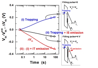
Understanding of the carrier capture-emission processes in the MOS gate structure is necessary to pave the way towards high-effective switching GaN transistors featuring MOS gate structure. Here, we developed a technique capable to separate carrier capture-emission processes by traps located in the oxide bulk and its interface with III-N heterostructure. For the separation, an original technique was used based on the threshold voltage transient monitoring in the MOS-HEMT structure as a function of temperatures and monochromatic light exposure in the energy range of 1.5 to 3.4 eV. We also analyzed in detail the impact of the gate structure properties on its capacitance behavior. Developed technique provides feed-back for technology development of highly-effective switching transistors based on GaN with MOS gate structure. The work was conducted within national APVV project and EU FP7 project HipoSwitch.
Ťapajna, M., Jurkovič, M., Válik, L., Haščík, Š., Gregušová, D., Brunner, F., Cho, E., and Kuzmík, J.: Bulk and interface trapping in the gate dielectric of GaN based metal–oxide–semiconductor high-electron mobility transistors. Applied Phys. Lett. 102 (2013) 243509.
- GaN/InAlN/AlN/GaN high-electron mobility transistors with Schottky-barrier gate and selectively etched access regions
Fabrication of unique InAlN barrier-based transistors with normally-off channel stem from the 7FP project MORGAN. Developed devices point on technologically simple method of designing Schottky-contact-based normally-off transistors with a high breakdown voltage and low leakage currents. Demonstrated transistors open a way towards robust high-power switches, as well as towards new generation of fast logic circuits. New technology is represented by a method of plasma etching of transistor access regions, which is highly selective and harmless to transistor performance. The concept was proposed and device processing was performed at the Institute of Electrical Engineering Slovak Academy of Sciences.
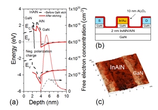
(a) Calculated energy band and electron concentration profiles at (GaN)/InAlN/AlN/GaN HEMT access regions before and after etching the GaN cap in equilibrium. (b) Sketch of the completed HEMT. (c) AFM image of etch test structure showing a 2.5 µm-wide etched window in the GaN cap.
Jurkovič, M., Gregušová, D., Palankovski, V., Haščík, Š., Blaho, M., Čičo, K., Fröhlich, K., Carlin, J., Grandjean, N., and Kuzmík, J.: Schottky-barrier normally off GaN/InAlN/AlN/GaN HEMT with selectively etched access region, IEEE Electron Dev. Lett. 34 (2013) 432-434.
Jurkovič, M., Gregušová, D., Haščík, Š., Blaho, M., Molnár, M., Palankovski, V., Donoval, D., Carlin, J.-F., Grandjean, N., and Kuzmík, J.: GaN/InAlN/AlN/GaN normally-off HEMT with etched access region. In: WOCSDICE-EXMATEC 2012. Proc. 36th European Workshop on Compound Semicond. Devices and Integrated Circuits and 11th Expert Evaluation & Control of Compound Semicond. Mater. and Technol. Eds. Y. Cordier and J.-Y. Duboz. Island of Porquerolles: CRHEA & CNRS 2012.
- Radical pn junction on GaP/ZnO nanorod
Core–shell GaP/ZnO nanowires (NWs) were prepared in a two-step process: (1) GaP NWs were grown on GaP substrate by low-pressure metalorganic vapour phase epitaxy using 30 nm Au seeds as nucleation centres, (2) the GaP NWs were covered in a thin nanocrystalline Ga-doped ZnO layer by sputtering in a Perkin Elmer planar RF diode system. Electrical contacts were processed to individual GaP/ZnO NWs using electron beam lithography, evaporation and lift-off of metallic layers: Au/Zn (GaP core) and Au/Al (ZnO shell). Electrical and photocurrent measurement of the NWs confirmed that a radial pn heterojunction was formed between the GaP core and ZnO shell.
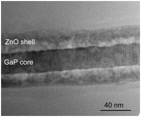
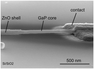
TEM cross-section of the GaP/ZnO core-shell nanowire (left) and SEM sideview of the contacted radial PN heterojunction (right)
Hasenöhrl, S., Eliáš, P., Šoltýs, J., Stoklas, R., Dujavová, A., and Novák, J.: Zinc-doped gallium phosphide nanowires for photovoltaic structures, Applied Surface Sci 269 (2013) 72-76.* IF: 2,11
Laurenčíková, A., Hasenöhrl, S., Eliáš, P., Stoklas, R., Blaho, M., Križanová, Z., and Novák, J.: Ohmic contacts to p-GaP/n-ZnO core/shell nanowires based on Au metallization, Applied Surface Sci 267 (2013) 60-64.* IF: 2,11
Novák, J., Križanová, Z., Vávra, I., Eliáš, P., Hasenöhrl, S., Laurenčíková, A., Novotný, I., Kováč, J., Šutta, P., and Mikulics, M.: Structural and optical properties of individual GaP/ZnO core-shell nanowires, Vacuum 98 (2013) 106-110. IF: 1,53
Novák, J., Eliáš, P., Hasenöhrl, S., Laurenčíková, A., Vávra, I., Novotný, I., Kováč, J., Mikulics, M., and Grünberg, P.: Properties of individual GaP/ZnO core-shell nanowires with radial PN junction. In: SPIE Microtechnologies 2013. Nanoeng.: Fabric., Propert., Optics, Devices X. Grenoble 2013, Proc. SPIE 8766 (2013) 8766-8.
2012
- N-Polarity InN/GaN/InAlN High-Electron-Mobility Transistors
There is a continuous effort to increase speed performance of III-V-based transistors. Among other limitations, which hinder transistor performance, there is a relatively high effective mass of electrons in the GaN channel. In our work, we propose and theoretically analyze transistors with a strained InN channel, which may increase transistor speed by 2.5 times. Transistor proposal takes into account possible technological problems of the growth; and thus it is proposed with N polarity. Consequently, InN channel can be grown as a last semiconductor layer which is insulated from the gate metal using a dielectric layer. In this way we expect to fill the “terahertz gap” between electron and photon devices.
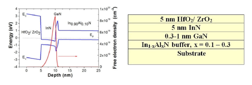
Calculated energy band-gap profile and epi-structure of the N-polarity InN/GaN/InAlN HEMT.
Kuzmik, J.: N-Polarity InN/GaN/InAlN High-Electron-Mobility Transistors, Applied Phys. Express 5, 044101 (2012). IF: 3,013
- A comprehensive analytical model for threshold voltage calculation in metal-oxide-semiconductor GaN heterostructure-field-effect-transistors
There is a great effort towards development of normally-off GaN heterostructure-field-effect transistor (HFET) for switching applications. Such technology can potentially have an enormous impact on the environment via minimizing the conversion losses in the electricity distribution and improvements in the hybrid cars technology. Among others, insulated gate HFETs, i.e. MOS-HFETs represent an excellent candidate for this purpose as an appropriate selection of the gate dielectric layer can provide a manipulation of the so-called surface donors, to allow the desired adjustment of the transistor’s threshold voltage (VT). Despite a fast development in this research field, a complete analytical model for the calculation and technological adjustment of VT was still missing in the literature. We proposed such a model together with separation of the relevant charges across the gate structure and explained the effect of the charges on MOS-HFET VT.
This work was carried out within the EU 7RP project HipoSwitch. The project aims the development and transfer of the technology of ‘normally-off’ power HFETs, i.e. devices with VT>0, for efficient power converters for telecom industry.
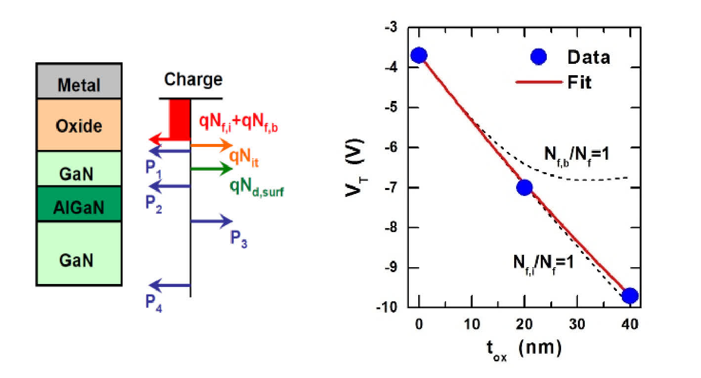
Ťapajna, M. and Kuzmík, J.: A comprehensive analytical model for threshold voltage calculation in GaN based metal-oxide-semiconductor high-electron-mobility transistors. Applied Phys. Lett. 100 (2012) 113509.
M. Ťapajna, K. Fröhlich, and J. Kuzmík, Int. Workshop on Semiconductor Devices – IWSD’12 (invited), March 5-6 2012, RCIQE, Sapporo, Japan.
M. Ťapajna and J. Kuzmík, In: Int. Workshop on Nitride Semicond., IWN’12, October 14-19 2012, Sapporo, Japan.
- Technology of nanorods for photovoltaic applications
Nanowires (NW) exhibit unique electrical and optical properties due to lowered dimensions and related confinement effects. An integration of these tiny objects necessitates better understanding of their individual intrinsic properties. Precise electrical characterization of NWs requests preparation of electrical nanocontacts with high stability, low contact resistance and ohmic behaviour. We applied a conventional field-effect transistor configuration that allows to estimate a type of conductivity and carrier mobility also. Structural properties of individual NWs were studied by means of SEM and TEM techniques. The GaP nanowires under study were grown on the p-type GaP (111)B substrate by a VLS technique using 30 nm colloidal gold particles as seeds. A part of NWs was covered by a thin ZnO layer (10 – 140 nm) deposited by RF sputtering. Deposition of thin ZnO layer on the GaP nanowire led to creation of radial PN junction in core-shell configuration. This work was done under support of APVV-0301-10 project.
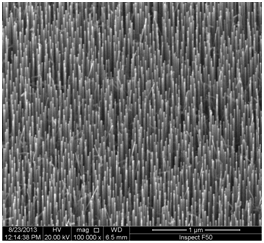
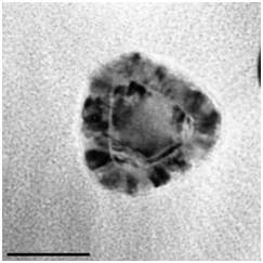
SEM sideview on forrest of GaP nanowires (left) and TEM micrograph (cross-sectional) shows the octahedral structure of a GaP NW core covered with the columnar structure consisted of ZnO grains. The scale bar represents 100 nm (right).
Novák, J., Novotný, I., Kováč, J., Eliáš, P., Hasenöhrl, S., Križanová, Z., Vávra, I., and Stoklas, R.: Preparation of thin Ga-doped ZnO layers for core-shell GaP/ZnO nanowires, Applied Surface Sci 258 (2012) 7607-7611.
Suslik, L., Pudis, D., Skriniarova, J., Kovac, J., Kubicova, I., Tvarozek, P., Martincek, I., and Novak, J.: GaAs/AlGaAs light emitting diode with 2D photonic structure in the surface, Proc. SPIE 8070 (2011) art. no. 807017
Novák, J., Šoltýs, J., Eliáš, P., Hasenöhrl, S., Stoklas, R., Dujavová, A., and Mikulics, M.: Electrical and photoluminescence properties of individual GaP nanowires doped by zinc, Phys. Stat. Solidi (a) 209 (2012) 2505-2512.
- Properties of GaAs-based transistors with in-situ AlOx passivation layer
The GaAs-based metal-oxide-semiconductor heterostructure field effect transistors (MOSHFET) represent alternative devices to conventional Si MOS transistors. However, performance of GaAs MOSHFETs is still hindered by a high density of surface/interface states. We studied GaAs MOSHFETs prepared with aluminium oxide as a passivation and gate insulator layer. Heterostructures with an InGaAs channel, AlGaAs barrier, and GaAs contact layer were grown on semi-insulating GaAs substrate by metal-organic chemical vapour deposition. The surface of GaAs was covered in-situ by a thin Al layer, which was subsequently oxidized at room temperature to obtain aluminium oxide. Static and microwave characteristics and capacitance measurements showed good device performances. The GaAs-based MOSHFETs yielded higher sheet charge density and saturation drain current compared to the counterparts without an oxide surface layer. For MOSHFET devices with 1,5 μm gate length, the current gain and unilateral power gain cut-off frequencies of fT=19GHz and fmax=48GHz were extracted, respectively. Our results indicate an efficient suppression of the trap states on the GaAs surface.
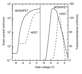
Static transfer(left) and transconductance (right) caharacteristics of the GaAs-based MOSHFET and HFETs
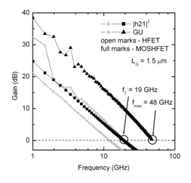
Small-signal microwave performance of the GaAs-based MOSHFET measured at VDS = 3 V and VGS=−3.8 V.
Kordoš, P., Kúdela, R., Stoklas, R., Čičo, K., Mikulics, M., Gregušová, D., and Novák, J.: Aluminum oxide as passivation and gate insulator in GaAs-basedfield-effecttransistorsprepared in situ by metal-organic vapor deposition. Applied Phys. Lett. 100 (2012) 142113.
Kordoš, P., Fox, A., Kúdela, R., Mikulics, M., Stoklas, R., and Gregušová, D.: GaAs-based metal-oxide-semiconductorfield-effecttransistorwithaluminum oxide gate insulatorprepared in situ by MOCVD. Semicond. SciTechnol. 27 (2012) 115002.
 Contact
 Intranet
 SK
SK

