Scanning Techniques Laboratory
Contact info: Ing. Šoltýs Ján, PhD.
Researchers in the Laboratory use both scanning electron as well as probe imaging techniques for complex analysis of physical properties of the surface. The combination of both equipments improves research outputs and extends the possibilities to examine various materials and structures. The laboratory allows scientists to image, characterize and even modify material structures in the range of few millimeters down to sub 100-nm scale.
Scope:
- Topography imaging of conductive and non-conductive samples
- Analysis of surface roughness
- Specialized magnetic measurements with external magnetic field
- Local anodic oxidation lithography
- Electron beam lithography
Equipment:
- NT-MDT NTegra scanning probe microscope (SPM) equipped with complementary probe techniques, including MFM, EFM, SFM and KPM
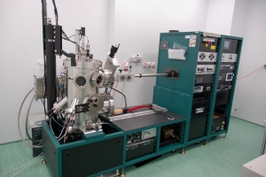
- FEI Inspect F50 scanning electron microscope (SEM) equipped with Elphy Quantum lithography software (Raith) and laser interferometric measuring system for precise stage positioning
- FEG 250 high resolution scanning electron microscope

Metal Deposition Laboratory
Contact info: Ing. Fedor Ján, PhD.
The laboratory is equipped with sputtering and evaporating machine ATC Orion 8E made by AJA International, Inc. The deposition system is placed in the clean room facility and it enables to deposit metals, insulators and magnetic materials on the samples with maximum diameter of 75 mm. It is used to work on projects related to microelectronics, nanotechnology, and modern environmental and medical sensors R&D.
Scope:
- Evaporation of materials by two independent electron guns
- AC and DC sputtering of metallic, insulating, and magnetic materials (co-sputtering, superlattice)
- Two in situ fed thermal evaporation sources
- Sample treatment: RF cleaning, ion beam cleaning, rotation and heating up to 850 °C
- Deposition of materials in different gas environment: N2 (TiN), O2 (Al2O3)
Raman Spektroscopy Laboratory
Contact info: Dr. rer. nat. Hulman Martin
Raman system by the WiTEC Company uses three lasers with wavelengths of 355, 532 and 785 nm for excitation of spectra. Laser light is a focused on a sample with a confocal microscope which also collects light scattered by the sample. The system uses three spectrometers equipped with CCD cameras, one optimised for each laser line. There is another spectrometer in the system used for luminescence measurements in the optical and near-infrared range up to 2.2 µm
Polarizers and analysers can be inserted in the optical path of the microscope allowing polarisation dependent measurements of Raman spectra. It is also possible to use a part with two Bragg gratings for measuring spectra very close to the excitation laser line down to 10 cm-1.
The system has a motorised table for xyz movement of the sample with a step well below 100 nm. Since the system allows measurement of the spectra with an integration time of less than 0.1 s, it is possible to measure several thousands of spectra in a reasonable time and construct a surface (2D) and spatial (3D) scans of a sample.

ALD laboratory
Contact info: Ing. Fröhlich Karol, DrSc.
Thin oxide films (Al2O3, TiO2, and HfO2) are prepared using atomic layer deposition. The films are grown using thermal, ozone, and plasma assisted modes at temperatures between ambient up to 350 °C. The films are used for insulation and passivation of the electronic devices (GaN and GaAs-based high electron mobility devices, HEMTs) and as active layers in memory elements based on resistive switching.
Scope:
- Deposition of thin oxide films with atomic level precision
- Growth of thin dielectric films with excellent properties at low temperatures
- Deposition on 3D substrates
- Modification of films and interfaces on atomic level
