Laboratory for X-ray optics and X-ray imaging techniques
Contact info: Ing. Zápražný Zdenko, PhD.
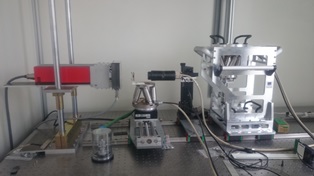
New X-ray laboratory for research, development, and testing of advanced X-ray imaging techniques (free-space propagation imaging, phase contrast, computerized tomography) equipped with micro-focus X-ray sources Hamamatsu, high performance X-ray camera miniFDI (Photonic Science) and high resolution rotary table (Newport) with full developed control software has been optimized (since 2015) also for development and testing of X-ray optical elements within the project “Research and development centre for advanced X-ray technology”. The optimization included the following enhancements: anti-vibration optical table, new cover system for X-ray radiation, Medipix detectors with two kinds of read-out chips (Si, GaAs), high-precision manipulators for X-ray optics consisting of two independent hexapods, a new control software allowing free programming (Python) of different types of experiments, resolution test pattern for testing of the spatial resolution down to 0.5 microns (X-radia X500-200-120), Fresnel zone plate (FZP) with a spatial resolution of 120 nm and focusing length of 30 cm (energy CuKα1).
Specifications:
- Micro-focus X-ray sources with a focal spot size of 8 microns: The source has a tungsten transmission anode and emits a conical X-ray beam with an output angle of 39 ° allowing geometrically enlargement of the sample up to 140-fold
- High resolution rotary table (minimal rotation step of 0.0002 °) with a sample holder allowing to capture sequential tomographic projections
- X-ray CCD miniFDI camera (Photonic Science). Basic parameters of the camera are as follows: pixel resolution of 1392 × 1040, pixel size: 6.4 × 6.4 μm2, active window: 10 x 8 mm2, scintillator: Gd2O2S: TB3with an optimal energy response from 5 keV to 17 keV
- Manipulator for X-ray optics consisting of two independent hexapods with angular resolution of 3.5 µrad and with minimal incremental axis motion (X, Y, Z) of 0.5 μm.
- Medipix detectors with two kinds of read-out chips (Si, GaAs). Pixel size: 55×55 μm2, active window: 14×14 mm2.
- Resolution test pattern for testing of the spatial resolution down to 0.5 microns
- (X-radia X500-200-120)
- Fresnel zone plate (FZP) with a spatial resolution of 120 nm and focusing length of 30 cm (for energy CuKα1)

Laboratory of MEMS Device Characterization
Contact info: RNDr. Haščík Štefan, PhD.
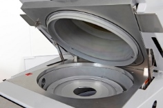
A fast and precise electro-thermo-mechanical characterization methods are needed to be developed to optimize a sophisticated technology of MEMS devices. The laboratory as established at the department for MEMS device characterization permits first of all the microchip to be packaged into the ceramic packages using a thermo-compression or ultrasonic bonding technique. There can be a various protective atmospheres (N2, H2, Ar, forming gas…) including the vacuum used for packaging of the MEMS devices. Precise dc measurements are performed in the wide temperature range (77 – 1000 K) at various ambient atmospheres using the semiconductor parameters analyzer (HP 4145B). In principle, there are possibilities to measure all the basic electro-thermal characteristics and parameters of the MEMS devices based on electro-thermal conversion mechanism (I-V characteristics, electro-thermal conversion characteristics, transfer characteristics, thermal resistance values, thermal time constant…) in situ at the ambient environment required, so their optimal operating conditions can easily be determined and analyzed. Sensing properties of MEMS gas sensors (sensitivity, selectivity, high temperature sensing ability and sensing time response) can be investigated using a chemical gas chamber (Fig. 1) up to 650 °C.

Fig. 1.: Chemical chamber for testing of sensing properties of MEMS gas sensors1
Contact: RNDr. Š. Haščík, PhD.
Plasma Etching Laboratory
Contact info: RNDr. Haščík Štefan, PhD.
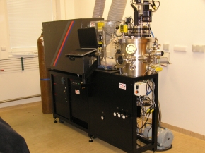
The Oxford Instruments – Plasmalab System100 is a state of the art tool for Inductively-Coupled Plasma Reactive Ion Etch (ICP RIE) processing of selected materials. Our research is primarily focused on etching of the GaN, AlGaN, InAlN, GaAs and InN semiconductors. The ICP RIE provides the etch precision and low damage selective reactive ion etching (SRIE) necessary to create next generation microscale (opto-)electronic devices and MEMS. A simple vacuum Load‑lock system is suitable for 4‑inch wafers as well as pieces which can be mounted on a handle wafer. ICP RIE equipment is operated by the control computer located in the clean room.
Scope:
- Etching of semiconductor materials and heterostructures based on GaN, AlGaN, InAlN, GaAs, and InN using the chlorine chemistry or its mixtures with fluorinated compounds
- Etching heterostructure layers (AlGaAs, GaAs, InGaAs, and InP) using SiCl4/Cl2, BCl3/Cl2, and Cl2/Ar
- Etching SiO2, Si3N4 and SiC by the CF4 and SF6 gases
Equipment:
Oxford Plasmalab 100 Inductively Coupled Plasma (ICP) etching system equipped with
- 13,6 MHz supply with automatic matching at the substrate electrode
- 3 kW Inductive Coupled Plasma (ICP 180) Source with electrostatic shielding
- temperature range substrate electrode: -30 + 80°C
- automatic 4-inch/100 mm wafer Load‑lock system
- PC Control with OPT PC2000 RIE Software under Windows 7
Laboratory of PLD
Contact info: Ing. Chromik Štefan, DrSc.
The laboratory enables the preparation of different thin films using pulsed laser deposition method. In this method, the laser beam vaporizes the surface of the target, producing a film with the same composition as the target. Due to high temperature of the evaporated material, low deposition temperature and smaller target area in respect to that of the substrate can be used.
Scope:
- Deposition of high-quality thin superconducting films at low substrate temperatures
- Deposition of multilayer structures in the same vacuum cycle with a fine control of the film thickness down to atomic monolayer
Clean Room Facility
Contact info: Ing. Kováčová Eva
The clean room facility is used to realize modern electronic devices and sensors. According to the US standard, the dust particle count is kept at 100 particles sized 0.5 µm and larger per cubic feet, which matches the levels in production facilities of producers of electronic circuits. The facility contains two rooms and is equipped with a Karl Suss MJB3 aligner, an optical microscope, deionized water source, two chemical boxes.

X-ray laboratory in Piešťany
Contact info: RNDr. Korytár Dušan, CSc.
Laboratory consists of two working places:
- X-ray diffrractometer HZG4 and double crystal camera DTS used to test quality of single crystals and for research and development of X-ray optical elements
- Recently built optical bench for research and development of modern X-ray imaging techniques (free space propagation, phase contrast, computer tomography) consisting of a microfocus X-ray source Hamamatsu, high resolution X-ray camera miniFDI (Photonic Science), and a Newport goniometer with complete developed controls
Technology laboratory in Piešťany
Contact info: RNDr. Boháček Pavol, CSc.
The laboratory is based on two high vacuum evaporation systems, clean room facility for photo-lithographic processing of semiconductor wafers to the 3″ diameter, and chemical boxes for etching of semiconductor wafers. The laboratory is used to work on research projects related to microelectronics, nanotechnology, and modern environmental sensors and radiation detectors. The layers and thin films are prepared using two different (co)deposition methods – thermal evaporation and electron beam evaporation and patterned by photo-lithography and wet etching.
Equipment:
- New high vacuum (HV) deposition equipment, model TFDS-462B from VST Services Ltd. with:
- Scroll pump and turbomolecular pump, 2.5×10⁻⁴ Pa in 50 min.,
- Electron beam evaporation source Telemark TT-6, 4 pocket × 4 cc, 6 kW (750 mA, 8 kV),
- Two thermal evaporation sources 3.2 kW (8 V, 400 A),
- Telemark 880 thin-film thickness and rate controller, 6 Mhz, accuracy ±0.5% of thickness,
- PC interface software communicates with PLC control system through Ethernet port
- Partially upgraded HV evaporation system with two electron guns and two thermal sources
- Chemical box for the work with organic and inorganic agents
- Heating and drying oven up to temperature 300° C for photoresist developing
- One-side optical mask aligner with optical microscope


