2023
Unidirectional spin-wave edge modes in a magnonic crystal
Over the past decade, the study of topological insulators has emerged as a vibrant area of interest across various physics disciplines, captivating researchers with their novel properties for foundational and practical applications. A hallmark characteristic of topological insulators is their unique structure: insulating internally while supporting conductive states on their surface. Specifically, in two-dimensional topological insulators, these conductive edge states are robust against scattering and propagate unidirectionally along the edge, positioning them as ideal candidates for data transport in next-generation computing devices. These unidirectional edge states have been observed experimentally across various systems, including electronic, acoustic and photonic crystals, and even in mechanical configurations such as rotating gyroscope networks. Notably, they all share a commonality where waves can traverse within these topological edge states.
Despite theoretical predictions made a decade ago about their presence in ferromagnetic systems—where spin (magnon) waves prevail—experimental verification of these states remains elusive. A significant hurdle has been the intricate geometry required for creating the proposed magnonic topological crystals. In our latest research, we introduce a design for a topological magnon crystal characterized by a simpler geometry, enhancing its feasibility for experimental realization and the observation of unidirectional edge states. Our design features a lattice of thin ferromagnetic squares, each bisected diagonally to form equal isosceles triangles. This structure’s simplicity, achievable by cutting a homogenous ferromagnetic layer along straight vertical, horizontal, and diagonal lines, markedly eases the fabrication process. Numerical simulations have demonstrated that when this magnonic crystal is subjected to a perpendicular magnetic field, spin waves are confined to propagate solely along its edges in a singular direction, which varies with the magnetic field’s magnitude.
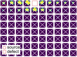
Numerical simulation of the DC edge state in our magnonic crystal. The red circle shows the place in the crystal where the spin wave is excited. Subsequently, the spin wave moves clockwise along the edge of the crystal and does not scatter in the opposite direction, even if it encounters a defect (red square).
Ref. Feilhauer, J., Zelent, M., Zhang, Z., Christensen, J., and Mruczkiewicz, M.: Unidirectional spin-wave edge modes in magnonic crystal, APL Mater. 11 (2023) 021104
2022
Magnetic Field Alignment and Optical Anisotropy of MoS2Nanosheets Dispersed in a Liquid Crystal Polymer
Our research focuses on developing an alignment methodology for 2D MoS2 ensembles and exploring the resulting anisotropic optical properties of these materials through photoluminescence and Raman spectroscopy.
Achieving orientational order in 2D nanomaterial assemblies or dispersions is crucial for leveraging their unique properties in practical applications. Nanocomposites consisting of anisotropic nanoparticles dispersed in liquid crystals (LCs) are particularly intriguing. They offer the promising ability to utilize the LCs’ stimuli-responsive director field to steer the nanoparticle alignment.
This study introduces a novel technique for magnetically orienting few-layer MoS2 nanosheets within a liquid crystalline polymer matrix. This process aligns the polymer’s director field—and consequently, the nanosheets—parallel to the applied magnetic field. The mesogens’ specific anchoring conditions facilitate the nanosheets’ alignment, positioning their surface normals perpendicular to the magnetic field. This unique orientation enables the examination of anisotropic optical properties in dispersed few-layer MoS2, a perspective previously difficult to attain. Specifically, it allows for investigating how the nanosheets’ edges and basal planes contribute differently to optical properties, such as photoluminescence, in MoS2. Our methodology provides a solid foundation for directly estimating the dichroic ratio in MoS2 photoluminescence.
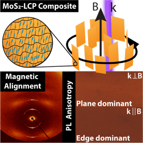
Ref. Uri R. Gabinet, Changyeon Lee, Na Kyung Kim, Martin Hulman, Sarah M. Thompson, Cherie R. Kagan, and Chinedum O. Osuji. Magnetic Field Alignment and Optical Anisotropy of MoS2 Nanosheets Dispersed in a Liquid Crystal Polymer. J. Phys. Chem. Lett. 2022, 13, 7994−8001
Project ATOPLOT
The project aimed to operationalize the concept of a 3D Atomic Layer Plotter, integrating Atomic Layer Deposition (ALD) technology with 3D printing. This innovative technology, developed by Atlant 3D Nanosystems—a Danish startup led by its founder and CTO, Ivan Kundrata, a PhD student—centres around a novel nozzle. This nozzle acts as a compact spatial ALD system, enabling the precise deposition of atomic layers by manoeuvring over the substrate, akin to ALD processes. The technology has been patented, with IEE SAV being one of the three patent holders.
IEE SAS’s contribution to the Atoplot project encompassed the conceptualization, design, and characterization of demonstrators. These simple microelectronic components showcased the plotter’s capabilities. IEE SAS manufactured these components using standard microelectronic techniques (lithography, Physical Vapor Deposition [PVD], ALD deposition, and shaping). The performance and quality of these traditionally fabricated components were then compared to those directly ‘printed’ by the plotter. The demonstrators included a temperature sensor utilizing a thin platinum layer, a capacitive distance sensor with thin-layer circular platinum electrodes, and a pressure sensor featuring a piezoelectric ALD ZnO layer.
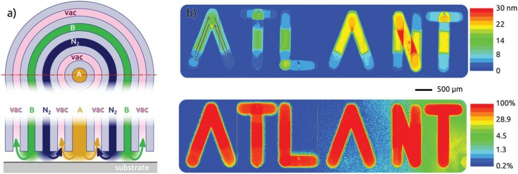
a) Microfluidic precursor delivery concept: Schematic view of the delivery nozzle in frontal view (top) and in cross‐section (lower panel). b) Demonstration of direct pattern generation by ALAM: Pt‐printed ATLANT logo featuring letters from A to T obtained with 140, 150, 170, 190, 200, and 210 individual passes, respectively. Top panel, imaging spectroscopic ellipsometry map of the Pt thickness on a linear scale. Lower panel, low‐energy ion scattering spectroscopy map presented on a logarithmic scale, yielding the element composition of the top atomic layer.
Ref. Kundrata, I., Barr, M.K.S., Tymek, S., Döhler, D., Hudec, B., Brüner, P., Vanko, G., Precner, M., Yokosawa, T., Spiecker, E., Plakhotnyuk, M., Fröhlich, K., and Bachmann, J.: Additive manufacturing in atomic layer processing mode, Small Methods (2022) 2101546
2021
New 2D material: CuI
Current 2D materials primarily derive from van der Waals (vdW)-layered bulk structures. However, only a limited number of such systems exist under ambient conditions and in total, only a few dozen 2D crystals have been successfully synthesised or exfoliated. One such material among countless predicted is the b-phase of CuI that is only stable at a narrow temperature range of 645-675 K. Therefore, exfoliation of monolayers from such crystals would be rather complicated.
This work demonstrates a method to stabilise a single layer of the high-temperature vdW-layered-CuI at ambient conditions by using graphene encapsulation. This new 2D material is synthesised directly between graphene layers in a single-step wet-chemical method. We comprehensively characterised its atomic configuration experimentally and confirmed the obtained heterostructure’s stability via density functional theory calculations.
The samples were synthesised in our lab and characterised by advanced electron microscopy techniques in Vienna, Tübingen and Antwerp. In the meantime, we have already applied the same process to produce 2D silver iodide (AgI) and nickel iodide (NiI2) crystals, and generalising this concept should allow access to other exotic layered structures, vastly expanding the currently available library of 2D materials.

a) A film of reduced graphene oxide (rGO) incorporating 2D h-CuI (the coin represents a scale). b) Bright-field TEM image of a single graphene/h-CuI flake suspended on a TEM support film. c,d) High-angle annular dark-field (HAADF) images of the flake edge. The orange and yellow contrast values in (d) are h-CuI. e) HAADF overview image of monolayer h-CuI crystals encapsulated in a bilayer graphene sandwich. No h-CuI contrast is visible on the monolayer area on the left-hand side. f) Atomically resolved HAADF closeup of a single 2D h-CuI crystal with a magnifying inset in the top right corner. g) Frequency domain representation of graphene outside the crystal, and h) that of the area demarcated by the dashed square on the crystal in (f) is shown. The solid circles in (g) indicate the visible first-order graphene reflections, superimposed on (h) using dashed circles. The images in (d–f) were false-coloured.
Ref.: Mustonen, K., Hofer, Ch., Kotrusz, P., Markevich, A., Hulman, M., Mangler, C., Susi, T., Pennycook, T.J., Hricovini, K., Richter, Ch. M., Meyer, J.C., Kotakoski, J., and Skákalová, V.: Towards Exotic Layered Materials: 2D Cuprous Iodide, Advanced Materials, doi: 10.1002/adma.202106922
Magnetic skyrmions in nanodisks
- M. Mruczkiewicz, I.V. Vetrova, J. Šoltýs, T. Šcepka, J. Dérer, R. Stoklas, V. Cambel
Magnetic skyrmions are topologically protected spin textures that currently attract considerable attention in fundamental and applied physics. We observed skyrmions in patterned nanodots fabricated by electron lithography and dry etching. The nanodots were composed of an ultrathin Pt/Co/Au multilayer, exhibiting the interfacial Dzyaloshinskii-Moriya interaction and a perpendicular magnetic anisotropy [1, 2]. In submicrometer dots with a diameter of 150–525 nm, we investigated the stabilization of various magnetic states, such as single-domain states, skyrmionic states, horseshoe-like domain structures, and worm-like domain structures. We have shown that a stack of six repetitions of Pt/Co/Au layers suffices to stabilize the skyrmion state inside a dot at room temperature. We demonstrate the process of skyrmion formation in nanodots by micromagnetic simulations [3]. We have found that the field generated by the sharp magnetic tip significantly affects the magnetization state of the nanodots and leads to the formation of skyrmions. The simulation explains the development of the magnetic state in the dot during magnetic force microscopy scans and confirms the possibility of skyrmion formation. The key transition in this process is the formation of the magnetic horseshoe domain.

Fig. Schematic representation of multilayer nanodot based on ultrathin Co layers placed between two different heavy metals: Au, Pt (left). An array of multilayer dots is scanned by MFM tip (middle), and its magnetic state is modified during the scan (right).
Outputs:
Vetrova, Iu.V., Zelent, M., Šoltýs, J., Gubanov, V.A., Sadovnikov, A.V., Ščepka, T., Dérer, J., Stoklas, R., Cambel, V., and Mruczkiewicz, M.: Investigation of self-nucleated skyrmion states in the ferromagnetic/nonmagnetic multilayer dot, Applied Phys. Lett. 118 (2021) 212409. (ITMS 313021T081, APVV-16-0068, 19-0311(RSWFA), VEGA 2/0160/19)
Zelent, M., Vetrova, Iu.V., Li, X., Zhou, Y., Šoltýs, J., Gubanov, V.A., Sadovnikov, A.V., Ščepka, T., Dérer, J., Stoklas, R., Cambel, V., and Mruczkiewicz, M.: Skyrmion formation in nanodisks using magnetic force microscopy tip, Nanomater. 11 (2021) 2627. (ERDF 313021T081, APVV 19-0311(RSWFA)), ERA.Net RUS Plus (TSMFA), VEGA 2/0160/19)
Vetrova, Iu.V., Šoltýs, J., Zelent, M., Sadovnikov, A.V., Gubanov, V.A., Ščepka, T., Dérer, J., Stoklas, R., Cambel, V., and Mruczkiewicz, M.: Investigation of the self-nucleated skyrmion states inside the ferromagnetic/non-magnetic multilayer dot. In: Sol-SkyMag 2021, virtual.
2020
Controlled motion of skyrmions in a magnetic antidot lattice
- J. Feilhauer, S. Saha, J. Tóbik, M. Zelent, L. J. Heyderman, and M. Mruczkiewicz
Magnetic skyrmions are robust defects in the out-of-plane magnetization of thin ferromagnetic layers where they can be moved by applying a spin polarized electric current. Due to the relatively low power required for their manipulation, skyrmions are promising candidates for the information carriers in the future efficient memory-storage devices and logical gates. However, spintronic devices based on skyrmions will require precise control of the skyrmion motion. We show that this goal can be achieved through the use of magnetic antidot array, i.e. square lattice of circular holes patterned in the ferromagnetic layer (see Fig.1). We perform micromagnetic simulations and semi-analytical calculations based on Thiele equation, where the skyrmion motion is driven by applied electric current. We demonstrate that an antidot array can guide the skyrmions in different directions depending on the parameters of the applied current pulse. Despite the fixed direction of the net driving current, due to the non-trivial interplay between the repulsive potential introduced by the antidots, the skyrmion Hall effect and the non-uniform current distribution, full control of skyrmion motion in a 2D lattice can be achieved. Moreover, we demonstrate that the direction of skyrmion motion can be controlled by tuning only a single parameter of the current pulse, i.e. current magnitude (see Fig.2).

Obr.1: Antidot lattice in the ferromagnet (CoFeB)/ heavy metal (HM) heterostructure with an example of current-driven skyrmion trajectory

Obr.2: Skyrmion trajectories in the antidot lattice for different magnitudes of applied current pulse
Outputs:
Feilhauer, J., Saha, S., Tóbik, J., Zelent, M., Heyderman, L.J., and Mruczkiewicz, M.: Controlled motion of skyrmions in a magnetic antidot lattice, Phys. Rev. B 102 (2020) 184425. (ERDF ITMS 313021T081, APVV-16-0068, 19-0311, Era.Net RUS Plus (TSMFA), VEGA 2/0162/18, 2/0150/18, UF, NSC, Poland UMO-2017/27/N/ST3/00419, No. UMO2018/30/Q/ST3/00416 and Nat. Scholarship Programme SR)
2019
Tailored growth of MoS2 few-layer films
Few-layer MoS2 films are promising candidates for applications in many areas, such as photovoltaics, photocatalysis, nanotribology, lithium batteries, hydrogenation desulfurization catalysis and dry lubricants, mainly due to their characteristic electronic, optical and catalytic properties. In general, two orientation options of the MoS2 layers are possible – horizontal (with the c-axis perpendicular to the plane of the substrate) and vertical (where the c-axis is parallel to the substrate), having different physicochemical properties. In the preparation of these materials by the sulfurization of molybdenum layers, the initial thickness of the molybdenum proved to be a critical parameter affecting the final orientation of the MoS2 layers. Unlike standard CVD chambers, where the reaction takes place in a two-zone furnace, we use a single zone furnace where we have a substrate and sulfur together at a high temperature in the center of the furnace. The aim of the work was to study the influence of other annealing parameters on the orientation of layers. The heating rate has been shown to be a critical parameter for the growth mechanism where rapid sulfurization leads to the growth of vertical MoS2 layers and slow sulfur evaporation leads to horizontal growth even for thicker initial molybdenum layers.


GIWAXS reciprocal space maps of MoS2 films on the c-plane sapphire substrate prepared from 3 nm thick Mo layers at 800 °C during 30 min with the heating rate of (a) 25 °C / min, (b) 5 °C / min and (c) 0.5 °C / min. The peaks at ~ 1 Å-1 originate from the (002) diffraction planes.
In addition, the single-zone sulfurization method used allowed the growth of MoS2 on the surface of the CVD microcrystalline diamond layers. This experimental design results in a sulfur-rich environment during the process, and diffusion of sulfur into molybdenum at temperatures below that required for formation of molybdenum carbide prevents the formation of the latter at the Mo-diamond interface. This finding may open a way for growing MoS2 layers on substrates which are otherwise susceptible to a chemical reaction with molybdenum. We have also shown that horizontal and vertical growth of the MoS2 layers is possible, depending on the thickness of the Mo layer as in the case of unstructured substrates. The combination of unique diamond properties and ultra-thin MoS2 layers with tunable crystallographic orientation can offer material properties relevant to a wide range of applications.


SEM images of MoS2 layers grown from (a) 1 nm, (b) 3 nm and (c,d) 6 nm thick Mo films deposited on the microcrystalline CVD diamond substrate. In (d), standing MoS2 flakes are seen on the edge of a diamond crystallite
Outputs:
Sojková, M., Végso, K., Mrkývkova, N., Hagara, J., Hutár, P., Rosová, A., Čaplovičová, M., Ludacka, U., Skákalová, V., Majková, E., Šiffalovič, P., and Hulman, M.: Tuning the orientation of few-layer MoS2 films using one-zone sulfurization, RSC Adv. 9 (2019) 29645-29651. IF 3.049, Q SJR 1
Sojková, M., Šiffalovič, P., Babchenko, O., Vanko, G., Dobročka, E., Hagara, J., Mrkývková, N., Majková, E., Ižák, T., Kromka, A., and Hulman, M.: Carbide-free one-zone sulfurization method grows thin MoS2 layers on polycrystalline CVD diamond, Sci Rep. 9 (2019) 2001. IF 4.011, Q SJR 1
2017
- Metadynamics
Knowledge of free energy barriers separating different states is critically important for assessment of long-term stability of information stored in magnetic devices. This information, however, is not directly accessible by standard simulations of microscopic models because of the ubiquitous time-scale problem, related to the fact that the transitions among different free energy minima have character of rare events. Here we show that by employing the metadynamics algorithm based on suitably chosen collective variables, namely helicity and circulation, it is possible to reliably recover the free energy landscape. We demonstrate the effectiveness of the new approach on the example of vortex nucleation process in magnetic nanodot with lowered spatial symmetry. With the help of reconstructed free energy surfaces (FES) we show the origin of the symmetry broken vortex nucleation, where one polarity of the nucleated vortex core is preferred, even though only in-plane magnetic field is present.

TÓBIK, Jaroslav – MARTOŇÁK, R. – CAMBEL, Vladimír. Free-energy landscapes in magnetic systems from metadynamics. In Physical Review B, 2017, vol. 96, r140413.
2016
- Spin Wave Excitations in Ultrathin Nanostructures with Dzyaloshinskii-MoriyaInteractionsThe dynamics of magnetization and spin wave excitations were studied in ultrathin ferromagnetic nanostructures with Dzyaloshinskii-Moriya interactions (DMI) present. This kind of exchange interaction is in focus of recent research, due to its contribution in magnetic skyrmion stabilization. The ultrathin magnonic crystal and arrays of isolated stripes were studied under the influence of uniform and point source magnetic field with the numerical methods. Large impact on the ferromagnetic resonance spectrum was shown and in result can bring a novel method for experimental estimation of DMI strength.Mruczkiewicz, M. and Krawczyk, M.: Influence of the Dzyaloshinskii-Moriya interaction on the FMR spectrum of magnonic crystals and confined structures, Phys. Rev. B 94 (2016) 024434.Mruczkiewicz, M., Gruszecki, P., Zelent, M., and Krawczyk, M.: Collective dynamical skyrmion excitations in a magnonic crystal, Phys. Rev. B 93 (2016) 174429.Mruczkiewicz, M. and Krawczyk, M.: Characterization of the spin wave properties in magnonic crystal films with Dzyaloshinskii-Moriya interactions. In: Sol-SkyMag 2016 – Inter. Conf. on Magnetism and Spintronics. San Sebastian 2016. (Talk)Mruczkiewicz, M., Krawczyk, M., and Guslienko, K.: Spin excitations over skyrmion state in magnetic dots. In: Sol-SkyMag 2016 – Inter. Conf. on Magnetism and Spintronics. San Sebastian 2016. (Poster)Mruczkiewicz, M. and Krawczyk, M.: Characterization of the spin wave properties in magnonic crystal films with Dzyaloshinskii-Moriya interactions. In: MANA 2016 – Micromagnetics: Analysis, Numerics, Applications. Wien 2016. (Poster)Mruczkiewicz, M., Gruszecki, P., Zelent, M., and Krawczyk, M.: Collective wave modes of dynamical skyrmions in magnonic crystal. In: MANA 2016 – Micromagnetics: Analysis, Numerics, Applications. Wien 2016. (Poster)
2015
- Magnetic states in nanomagnets with broken symmetry
In this work we study magnetic states in ferromagnetic objects by simulations and experimentally, too. In the theoretical part we explore the nature of the magnetic state in nanoobjects [1]. The dynamics of the magnetic state of the objects with lowered symmetry shows asymmetric time evolution, which we explain by a single-spin model. Such simplified model is opening a possible venue for controlling magnetic states of the future nanodevices in practical applications. In the experimental part we have: a) developed novel scanning method, dual-tip magnetic force microscopy (DT-MFM), b) explored magnetization reversal of the nanomagnet using micro-Hall probe magnetometry [3]. The DT-MFM imaging [2] uses two tips, one (non-magnetic) evaluates topology of the nanomagnet and the second one its magnetic field. The magnetic tip never touches the magnetic surface, so the perturbations introduced by the magnetic tip are minimized using this method. The Hall-probe magnetometry showed how the dynamics of the magnetic state of the nanomagnet depends on the angle of the external field and the temperature.

Standard tip (left) perturbs magnetic vortex in Py ellipse while dual tips gives correct image
[1] Tóbik, J., Cambel, V., and Karapetrov, G.: Asymmetry in time evolution of magnetization in magnetic nanostructures. Sci Reports 5 (2015) 12301.
[2] Precner, M., Fedor, J., Šoltýs, J., and Cambel, V.: Dual-tip magnetic force microscopy with suppressed influence on magnetically soft samples. Nanotechnol. 26 (2015) 055304.
[3] Ščepka, T., Polakovič, T., Šoltýs, J., Tóbik, J., Kulich, M., Kúdela, R., Dérer, J., and Cambel, V.: Individual vortex nucleation/annihilation in ferromagnetic nanodots with broken symmetry observed by micro/Hall magnetometry. AIP Adv. 5 (2015) 117205.
2014
- Resistive switching in TiO2– and HfO2-based structures prepared by atomic layer deposition
Resistive switching in metal-insulator-metal structures is a challenging topic for application in future random access memories (RAM). In our papers we have shown that TiO2 and HfO2 structures prepared using ALD technology are suitable for resistive switching effect. To achieve bipolar resistive switching, one has to use electrode with different output work functions and affinity to oxygen, e.g. TiN and Pt. In the case of HfO2based structures, the resistive switching effect was observed also for ultrathin layers of thickness ~ 2 nm. We have found that forming voltage of such structures depends on the HfO2 thickness. Characterization of the structures using pulsed voltage (pulse length 1 µs), 108 switches with resistivity ratio higher than 10 for reading voltage 0,2 V. Such characteristics show that HfO2 based structures are perspective for future RAM memories.
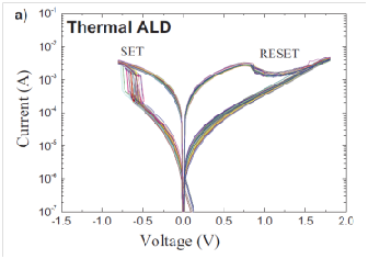
Fig. Resistive switching loops of the Pt/HfO2/TiN structures with the HfO2 layer deposited by thermal assisted ALD.
Publikácie:
B. Hudec, A. Paskaleva, P. Jančovič, J. Dérer, J. Fedor, A. Rosová, E. Dobročka, K. Fröhlich: Resistive switching in TiO2-based metal-insulator-metal structures with Al2O3 barrier at the metal/dielectric interface, Thin Solid Films 563 (2014) 10.
P. Jančovič, B. Hudec, E. Dobročka, J. Dérer, J. Fedor, K. Fröhlich: Resistive switching in HfO2-based atomic layer deposition grown metal-insulator-metal structures, Appl. Surf. Science 312 (2014) 112.
- Visualizing domain wall and reverse domain superconductivity
In magnetically coupled, planar ferromagnet-superconductor (F/S) hybrid structures, magnetic domain walls can be used to spatially confine the superconductivity. In contrast to a superconductor in a uniform applied magnetic field, the nucleation of the superconducting order parameter in F/S structures is governed by the inhomogeneous magnetic field distribution. The interplay between the superconductivity localized at the domain walls and far from the walls leads to effects such as re-entrant superconductivity and reverse domain superconductivity with the critical temperature depending upon the location. Here we use scanning tunnelling spectroscopy to directly image the nucleation of superconductivity at the domain wall in F/S structures realized with Co-Pd multilayers and Pb thin films. Our results demonstrate that such F/S structures are attractive model systems that offer the possibility to control the strength and the location of the superconducting nucleus by applying an external magnetic field, potentially useful to guide vortices for computing application.
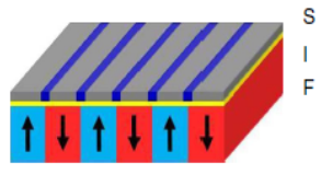
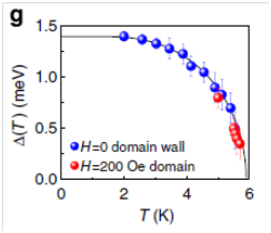
Fig. (left) Schematics of a hybrid system, consisting of a ferromagnet (F), insulator (I) and a superconducting film (S). (right) Temperature dependence of the gap values obtained from the conductance spectra. The experimental points are compared with the BCS gap equation (solid line).
Iavarone, M., Moore, S.A., Fedor, J., Ciocys, S.T., Karapetrov, G., Pearson, J., Novosad, V., and Bader, S.D.: Visualizing domain wall and reverse domain superconductivity, Nature Comm. 5 (2014) 4766.
- Fast highly-sensitive semiconductor gas sensor based on the nanoscale Pt–TiO2–Pt sandwich
Development of fast highly-sensitive semiconductor gas sensors operating at room temperature, which would be compatible with semiconductor technology, remains a challenge for researchers. Here we present such sensor based on a nanoscale Pt–TiO2–Pt sandwich. The sensor consists of a thin (∼30 nm) nanocrystalline TiO2layer with ∼10 nm grains, placed between the bottom Pt electrode layer and top Pt electrode shaped as a long narrow (width w down to 80 nm) stripe. If we decrease w to ∼100 nm and below, the sensor exposed to air with 1% H2 exhibits the increase of response (Rair / RH2) up to ∼107and decrease of the reaction time to only a few seconds even at room temperature. It is shown theoretically, that the sensitivity increase is due to a nontrivial non-ohmic effect, a sudden decrease (by three orders of magnitude) of the electrical resistance with decreasing w for w ∼ 100 nm (see Fig.). This non-ohmic effect is explained as a consequence of two nanoscale-related effects: the hydrogen-diffusion-controlled spatially-inhomogeneous resistivity of theTiO2layer, combined with onset of the hot-electron-temperature instability when the tiny grains are subjected to high electric field.
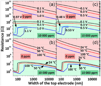
Fig. : Sensor resistance as a function of the top electrode width.
Plecenik, T., Moško, M., Haidry, A., Durina, P., Truchly, M., Grančič, B., Gregor, M., Roch, T., Satrapinskyy, L., Mošková, A., Mikula, M., Kúš, P., and Plecenik, A.: Fast highly-sensitive room-temperature semiconductor gas sensor based on the nanoscale Pt-TiO2-Pt sandwich. Sensors Actuators B 207 (2015) 351-361.
2013
- Switching-magnetization Magnetic force microscopy with high spatial resolution
Basic drawback of standard magnetic force microscopy (MFM) is its relative low spatial resolution on the level of ~ 20 nm. Improvement of the resolution is limited by the mixing of magnetic and van der Waals forces for scanns closer than 20 nm above the sample. We have solved the problem by introducing a novel scanning method, so called Switching-magnetization MFM method (SM-MFM). Within the method two scans of the sample are realized with opposite tip polarity, switchd by the external magnetic field. Then the data addition of these scans gives van der Waals forces, and their difference gives magnetic image of the sample. The SM-MFM method thus separates atomic and magnetic forces in scans realized in close proximity above the sample (e.g. 5 nm). Therefore it improves the spatial resolution of the MFM method below 10 nm, which is important for novel feromagnetic memories. High spatial resolution is documented in the figure achieved using the SM-MFM method.
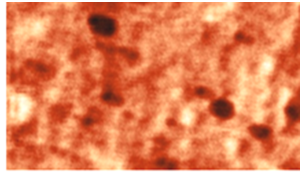
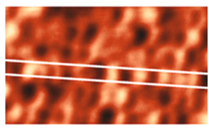
Fig.: Left is topography, right image of magnetic forces of the HDD memory (625 Gb/inch2) achieved by the SM-MFM method. Bit dimension is 25 x 40 nm2, figure dimensions are 500 x 800 nm2.
1. Cambel, V., Precner, M., Fedor, J., Šoltýs, J., Tóbik, J., Ščepka, T., and Karapetrov, G.: High resolution switching magnetization MFM, Applied Phys. Lett. 102 (2013) 062405.
2. J. Fedor et al, ISPM Conf 2013, Dijon; V. Cambel et al, MRS Spring Meeting, San Francisco, USA; M. Precner et al, CSMAG, Kosice 2013. Talks.
- Magnetization and vortex phase diagram in CuxTiSe crystals
CuxTiSe2 is a recently found material in which compete superconductor and charge density wave states for interval 0.04 < x < 0.06. We have extracted several important parameters from magnetization reversal characteristics of several crystals with various concentrations of Cu. Superconductive anisotropy is very low, close to 1.7, and independent on doping level. But, it is enhanced for weakly doped crystals. We assume that this is due to the competition between superconductivity and the charge density wave state. From the magnetization curves we have extracted also extremely low SC current densities, which is the consequence of very low intrinsic pinning. Surprisingly looks also the phase diagram of the SC vortices with extremely wide liquid phase. This is non-typical result for low-temperature superconductor with low anisotropy. We explain it as a consequence of already mentioned small pinning.
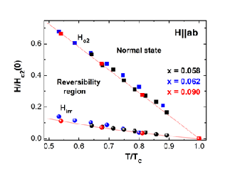
Fig.: Figure shows wide reversibility region of the SC vortices
1. Barančeková Husaníková, P., Fedor, J., Dérer, J., Šoltýs, J., Cambel, V., Iavarone, M., May, S., and Karapetrov, G.: Magnetization properties and vortex phase diagram of CuxTiSe2 single crystals. Phys. Rev. B 88 (2013) 174501.
2. Kačmarčík, J., Pribulová, Z., Paľuchová, V., Szabó, P., Barančeková Husaníková, P., Karapetrov, G., and Samuely, P.: Heat capacity of single-crystal CuxTiSe2 superconductors. Phys. Rev. B 88 (2013) 020507.
3. P. Husaníková et al, March Meeting 2013, Baltimore, Maryland, USA. Z. Pribulová et al, March Meeting 2013, Baltimore, Maryland, USA. Talks.
2012
- Dynamics of magnetic vortices in ferromagnetic nanoelements for nonvolatile memories
We study theoretically and experimentally magnetic effects in ferromagnetic nanoelements. Such nanomagnets are perspective for future nonvolatile high-density memories. Each of the designed nanomagnet can store two bits, polarity and chirality. An important condition for the designed element is the simplicity of the read/write process. We show that the shape of the nanomagnet influences significantly the read/write processes, and the simplest one appears for the objects with broken symmetry, namely for so called „Pacman-like“ (PL) shape. Micromagnetic simulations show that all four ground states of the nanomagnet can be easily achieved by switching of the in-plane external field in the defined direction according the symmetry axes of the nanomagnet. In the experimental part of the work we have prepared PL memory elements of the diameter of 200 and 300 nm, and also elements on a micro-Hall probe. The experiments support the vortex dynamics obtained by the micromagnetic simulations. The challenge of the next experiments is to fabricate ferromagnetic nanoelements of the diameter lower than 100 nm and use them as the basis of the nonvolatile memory.
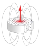
Fig.: „Pacman-like“ nanomagnet
1. V. Cambel and G. Karapetrov, Control of vortex chirality and polarity in magnetic nanodots with broken rotational symmetry, Phys. Rev. B 84 (2011) 014424.
2. J. Tóbik, V. Cambel, and G. Karapetrov: Dynamics of vortex nucleation in nanomagnets with broken symmetry, Phys. Rev. B 86 (2012) 134433.
3. Cambel, V. and Karapetrov, G.: Micromagnetic simulations of pac-man-like nanomagnets for memory applications. J. Nanosci Nanotechnol. 12 (2012) 7422-7425.
4. Šoltýs, J., Gaži, Š., Fedor, J., Tóbik, J., Precner, M., and Cambel, V.: Magnetic nanostructures for non-volatile memories. Microelectr. Engn. 110 (2013) 474-478.
5. Cambel, V., Tóbik, J., Šoltýs, J., Fedor, J., Precner, M., Gaži, Š., Karapetrov, G., : The influence of shape anisotropy on vortex nucleation in Pacman-like nanomagnets. J. Magnetism Magnetic Mater. 336 (2013) 29-36.


