2024
InN/InAlN heterostructures for new generation of fast electronics
In this work, we prepared InN/In0.61Al0.39N-based heterostructures with nitrogen (N) polarity by chemical vapor deposition of organometallics directly on a sapphire substrate. The thickness of the InN layer was 20 nm and that of the InAlN layer was 340 nm. During the growth of such a structure, we tested the effect of a thin AlN layer sandwiched between InN and InAlN, prepared at 710 °C for 35 s. This layer served as an interlayer to separate the underlying InAlN layer and the InN channel or as part of the nucleation of the underlying InAlN layer after nitridation of the sapphire substrate. High-resolution transmission electron microscopy imaging revealed that when AlN was used as the interlayer, the interlayer was only approximately two atomic layers thick. In this case, we observed an improvement in the form of a reduction in the concentration of screw and edge dislocations in the partially strained InN layer to 6.5 × 10⁹ and 38 × 109 cm-2, respectively. With the use of this AlN interlayer, we also achieved suppression of electron scattering caused by the so-called distant donor lattice disorder typical of ternary compound semiconductors. This step allowed us to achieve high mobility and electron concentration in InN at 620 cm2/Vs and 3×1013 cm-2 at room temperature. Using electrical measurements using ultrashort pulses of 10 ns on fabricated test resistors, we demonstrated a current density of 12-16 A/mm, a breakdown electric field of ~75 kV/cm, and an electron drift velocity of ~2×107 cm/s for the InN layer, bringing us closer to practical components capable of operating at ultra-high, sub-THz frequencies at room temperature.
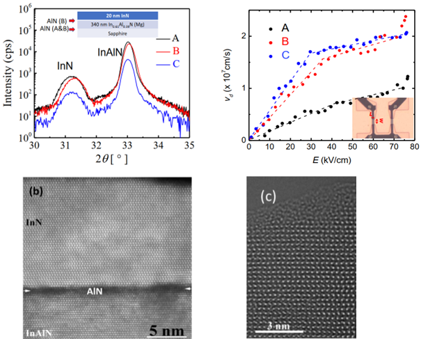
X-ray diffraction pattern for 20 nm thick InN layers on Mg-doped In0.61Al0.39N substrate grown on sapphire substrate (left), achieved electron drift velocity determined from measurements on test resistors (right), high-resolution transmission electron microscope image showing InN/AlN/InAlN quantum well section and detail of N polarity of the prepared structure (bottom).
Improved thermal performance of InGaAs/GaAs nanomembrane HEMTs transferred onto various substrates by epitaxial lift-off
In this joint study with Wuhan and Slovak University of Technology, we focused on innovation in the field of high electron mobility transistors (HEMT) prepared from GaAs semiconductor. These components are particularly key in high-frequency wireless communication applications in consumer, defense and space applications, as well as in quantum computing technology, which relies heavily on the use of compound semiconductor-based amplifiers. These enable high-frequency, low-noise operation even at cryogenic temperatures, essential for faithful amplification of weak qubit states. In this study, we have documented the enhancement of thermal transport properties of GaAs nanomembranes transferred from pristine GaAs substrate to foreign substrates (sapphire, Si and SiC) with different thermal conductivity. Such nanomembranes form the base layer of the structure from which the transistor is later fabricated. To separate the nanomembranes from the original substrate, a technique called epitaxial lift-off (ELO) was used. These formed a mechanical bond on the foreign substrate using van der Waals forces. For the thermal characterization of the nanomembranes, a non-destructive optical method called transient thermoreflectance (TTR) was used, which was combined with an electrothermal simulation of the complete GaAs HEMT component to verify the improvement of its properties. The simulation was extended to include a diamond substrate. This physical simulation showed a significant decrease in self-heating and thermal resistance of the components (Rth) up to ~30% when SiC and diamond substrate were used. At the same time, the simulations suggest that optimizing the interface between GaAs and the substrate could further reduce the operating temperature of the components, ideally by as much as 29-41%. These results confirm the potential of ELO technology, as components prepared on the transferred nanomembranes once they have been molded can provide higher performance while maintaining all their operational properties and without the risk of overheating. The research also highlights the economic potential of SiC substrates, which are both more affordable and more dimensional than diamond, while still providing similar benefits in terms of improved heat dissipation. In addition, the use of ELO technology enables the reuse of GaAs substrates, thereby reducing manufacturing costs and increasing the sustainability of the production process.
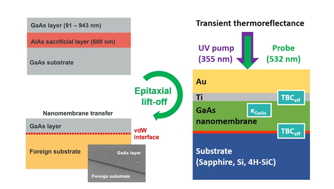
Schematic illustration of the ELO technique – separation of a GaAs nanomembrane and its transfer to a foreign substrate (left) and schematic cross-section of the structure used to measure the thermal properties (right).
Foreign partner: Institute of Technological Sciences, Wuhan University, China
International project: APVV SK-CN-21-0013, Vlastnosti tepelného transportu v budúcich perspektívnych polovodičových materiáloch a rozhraniach/Thermal transport properties of perspective future semiconductor materials and interfaces (responsible F. Gucmann).
Publication: Gucmann, F., Meng, B., Chvála, A., Kúdela, R., Yuan, C., Ťapajna, M., Florovič, M., Egyenes, F., Eliáš, P., Hrubišák, F., Kováč, J.Jr., Fedor, J., and Gregušová, D. Improved thermal performance of InGaAs/GaAs nanomembrane HEMTs transferred onto various substrates by epitaxial lift-off, ACS Applied Electron. Mater. 6 (2024) 5651–5660.
2023
Vertical GaN transistor with semi-insulating channel
GaN-based power electronics is becoming vital for an efficient energy conversion. Here, vertical device geometry is essential for reducing parasitic effects like self-heating and surface trapping. We demonstrate a novel simplified concept of vertical GaN transistors having C-doped 1.3-mm thick semi-insulating (SI) channel layer. Structures were grown using a metal organic chemical vapor deposition on conductive GaN substrates. SI GaN is sandwiched between 2.5-mm thick n-GaN drift layer and a top n-GaN contact layer. The gate contact formed on the mesa sidewall is insulated from the vertical channel using Al2O3 grown by an atomic layer deposition. Robust lay-out of the device, missing p-type doping, perspective scalability of the breakdown voltage without compromising n-type doping in the drift region and high electron mobility in the channel are the main assets of the approach. Our study provides an impetus for further development.
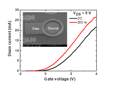
Transfer characteristics of the vertical GaN transistor in the dc, 100 and 200 ns gate-pulse operation. Inset shows processed device with a diameter of 180 mm.
Šichman, P., Stoklas, R., Hasenöhrl, S., Gregušová, D., Ťapajna, M., Hudec, B., Haščík, Š., Hashizume, T., Chvála, A., Šatka, A., and Kuzmík, J.: Vertical GaN transistor with semi-insulating channel, Physica Status Solidi (a) 220 (2023) SI2200776.
J. Kuzmik: Vertical GaN transistor with insulating channel and the method of forming the same, Slovak patent No. 289027 (granted), European patent pending no. EP18830014.9.
Growth of InAlN layers with high In N-polarity by chemical vapor deposition from organometallics on diverted and non-diverted sapphire substrates
In this work, we used the metalorganic chemical vapour deposition (MOCVD) method to prepare InAlN layers with high indium and N-polarity directly on sapphire substrates not deflected from the c-plane or deflected from the c-plane by 4° towards the a-plane, and monitored the change in the material properties of InAlN with respect to the change in the selected growth flow rate of the In precursor (trimetylindium, TMIn) in the range of 8.42-13.48 μmol/min. With increasing TMIn flow rate, we observed an increase in the In content of InAlN layers up to 55 – 69% regardless of the sapphire substrate deflection. For less than 63% In content, we obtained a reduction of crystalline defects on undiverted substrates; however, the use of diverted substrates resulted in lower surface roughness of the InAlN layers. With these findings, we confirmed the suitability of N-polar InAlN layers with high In content as a suitable tailoring layer for new types of heterostructure microelectronic components.
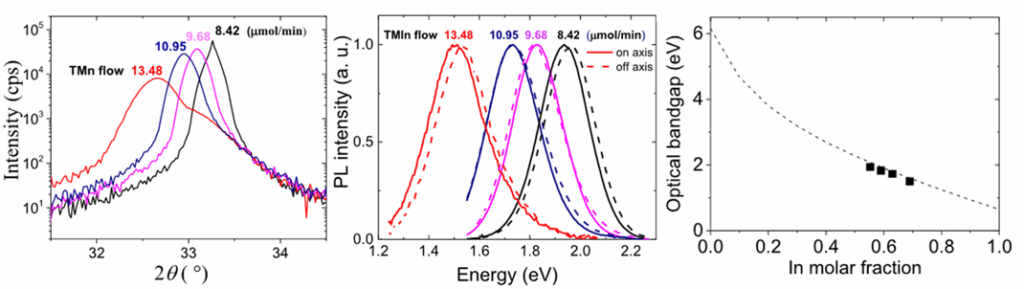
X-ray diffraction pattern (left) and photoluminescence spectra (middle) for InAlN layers prepared at different In precursor flow rates. Calculated InN optical forbidden band energy values for different indium content (right).
Project: VEGA 2/0005/22 (Responsible J. Kuzmík)
Hasenöhrl, S., Blaho, M., Dobročka, E., Gucmann, F., Kučera, M., Nádaždy, P., Stoklas, R., Rosová, A., and Kuzmík, J.: Growth of N-polar In-rich InAlN by metal organic chemical vapor deposition on on- and off-axis sapphire, Mater. Sci Semicond. Process. 156 (2023) 107290.
Heteroepitaxial growth of Ga2O3 on 4H-SiC by liquid-injection MOCVD for improved thermal management of Ga2O3 power devices
In this study, we have addressed the integration of a novel Ga₂O₃ semiconductor with SiC substrates in order to optimize the thermal performance of power Ga₂O₃ devices. The main advantage of Ga₂O₃ is its high theoretical breakdown field and wide band gap. The high breakdown field potentially enables the use of Ga₂O₃ for high voltage components, while the wide band gap opens up the possibilities of its use for optoelectronic components operating in the deep UV region. Ga₂O₃ has several crystalline phases, of which β-Ga₂O₃ and κ-Ga₂O₃ were investigated in this case.
One of the main drawbacks of Ga₂O₃ is its low thermal conductivity, which presents a limitation to the power range as well as the lifetime of Ga₂O₃-based components. It is the issue of low thermal conductivity and possible alternative solutions that we address in this publication. We have attempted to address this problem by growing Ga₂O₃ layers on SiC substrates with high thermal conductivity. Based on a combination of thermal measurements and simulation, we found that the placement of thin Ga₂O₃ layers on SiC allows for a significant reduction of transistor self-heating compared to components prepared on Ga₂O₃ substrates (up to almost 30× for thicknesses < 2 µm) and also that no significant thermal barrier is formed between the Ga₂O₃ layers and the SiC substrate, which would fundamentally hinder the dissipation of the lossy heat.
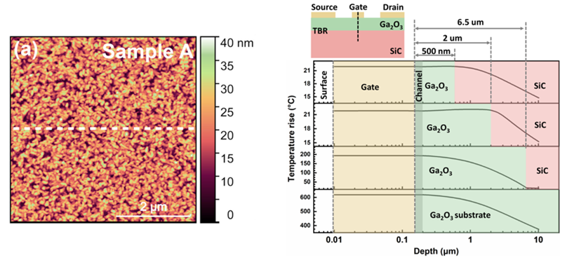
Ga₂O₃ layer surface imaged by atomic force microscope (left) and the result of simulation of self-heating depletion field-effect transistor (MOSFET) fabricated from our prepared Ga₂O₃ layers on SiC (right). The simulation shows that while maintaining a channel thickness of 2 μm, the self-heating of the component is imperceptible compared to higher thicknesses or the case of a typically used Ga₂O₃ substrate instead of SiC.
Hrubišák, F., Hušeková, K., Zheng, X., Rosová, A., Dobročka, E., Ťapajna, M., Mičušík, M., Nádaždy, P., Egyenes, F., Keshtkar, J., Kováčová, E., Pomeroy, J.W., Kuball, M., and Gucmann, F.: Heteroepitaxial growth of Ga2O3 on 4H-SiC by liquid-injection MOCVD for improved thermal management of Ga2O3 power devices, J. Vacuum Sci Technol. A 41 (2023) 042708. 2.9 – IF, Q2 – JCR
2022
In(Ga)N 3D growth on GaN-buffered on-axis and off-axis (0001) sapphire substrates by MOCVD
Recent advances in the epitaxial growth of indium nitride layers opened new horizons for photonic and electronic devices. In our group we studied the growth of self-assembled InN nano-sized pyramids on GaN-buffered sapphire substrates with two different surface inclinations. A continuous layer of small In(Ga)N conical pyramids (~10-25 nm height) in which large conical pyramids with the approximate height of 50-80 nm were obtained. The low temperature photoluminescence spectra showed a single maximum at 853 meV with a full width at half maximum (FWHM) of 75 meV and 859 meV with a FWHM of 80 meV for the off-axis and on-axis samples, respectively.
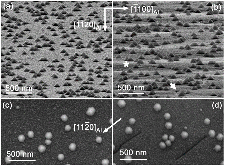
SEM images of the In(Ga)N layers grown on the on-axis (a, c) and off-axis (b, d) GaN/Al2O3 substrates. (a) and (b) images were taken with sample tilted by 85° from the surface normal; (c) and (d) are the plane-view images oriented according to the shown direction of Al2O3 substrate. The asterisk in (b) denotes clearly visible steps related to the off-axis substrate; the thick short arrow points to one of the observed cracks.
Rosová, A., Dobročka, E., Eliáš, P., Hasenöhrl, S., Kučera, M., Gucmann, F., and Kuzmík, J.: In(Ga)N 3D growth on GaN-buffered on-axis and off-axis (0001) sapphire substrates by MOCVD, Nanomater. 12 (2022) 3496. IF 5.72, Q 1.
2021
InN: breaking the limits of solid-state electronics
InN has been predicted to be among the top candidates for materials with the highest electron velocity. However, this theoretical prediction has not been validated yet. In the present work, we demonstrate state-of-the art InN material with an electron drift velocity of about 1 × 108 cm s-1 at an electric field of 48 kVcm-1. This is the highest steady-state electron velocity ever measured in any solid-state device. Even more, our experimental value outperforms theoretical predictions by a factor of two suggesting a need for revised understanding of InN fundamental properties. If technology of InN-channel transistors is fully developed, present THz frequency gap between the electronic and optical devices will be erased.
This work has been performed in collaboration with University of Crete and MRG IESL Crete.

Current-voltage characterization and electron velocity extraction of InN resistors. (a) Typical 10-ns long current-voltage waveform. Rise and falling time was about 6 ns. To construct current-voltage characteristics shown in (b), waveforms were averaged over 2-ns time span around the peak. Sketch of the measurements set-up is depicted in the inset. HP 8114A 100 V/2 A was used as a programmable pulse generator, Rm = 8.5 W. (b) Current density dependence on the applied electric field (left-side axis) and corresponding extracted electron drift velocity (right-side axis) on a series of resistors. Dash lines interpolate the values. Inset shows optical microscope view of two 8-mm long and 4-mm wide InN test resistors. Non-alloyed Ti/Al/Ni/Au ohmic contacts and bottom GaN surface exposed by dry etching are clearly distinguishable.
J. Kuzmík, A. Adikimenakis, M. Ťapajna, D. Gregušová, Š. Haščík, E. Dobročka, K. Tsagaraki, R. Stoklas, A. Georgakilas: InN: breaking the limits of solid-state electronics, AIP Advances 11 (2021) 125325.
2020
Growth and Properties of N-polar InN/InAlN Heterostructures
InN has been reported as a promising material for ultra-high frequency transistors. This was particularly because of theoretically predicted record electron drift velocity, highest from all common semiconductors. However, no microwave InN-channel transistor has been demonstrated till now. It can be suggested that the In-rich InAlN buffer layer can reduce density of dislocations in InN by providing lower lattice mismatch if compared with more common growth on GaN. Consequently, in N-polar InN/InAlN heterostructure we could demonstrate decent electron mobility of 720 cm2V-1s-1 with InN layer as thin as 20 nm. Because of improved InN crystalline quality, Hall data of the N-polar InN/InAlN heterostructure grown on on-axis sapphire was superior to the ones on off-axis sapphire. Further improvement of the mobility beyond the present state-of-the art can be obtained by InAlN surface smoothing, In molar fraction increase and by compensating InAlN unintentional doping. In our work we show viable steps towards InN-channel HEMTs.

a) XRD 2θ/ω diffraction curve of InN(20 nm)/In0.57Al0.43N heterostructure grown on on-axis sapphire, b) 2D and 3D views of 2×2 µm2 AFM scans of 20 nm thick InN grown on N-polar In0.57Al0.43N layer, c) InN electron mobility and concentration dependence on InN thickness.
Hasenöhrl, S., Dobročka, E., Stoklas, R., Gucmann, F., Rosová, A., and Kuzmík, J.: Growth and Properties of N-polar InN/InAlN Heterostructures, Phys. Stat. sol (a) 217 (2020) 2000197.
Kučera, M., Hasenöhrl, S., Dobročka, E., Rosová, A., Eliáš, P., Gucmann, F., and Kuzmík, J.: Morphology, crystalline quality, and optical properties of MOCVDgrown InN/InAlN heterostructures. In: ASDAM 2020. Eds. T. Izsák et al. IEEE 2020. ISBN 978-1-7281-9776-0. P. 131-134.
2019
2018
2017
2016
2015
2014
- Technology transfer of normally-off AlGaN/GaN HEMTs to Ferdinand Braun Institute Berlin
- Design optimization of high-power AlGaN/GaN HEMT switches
- InGaAs/GaAs metal-oxide-semiconductor heterostructure field-effect transistors with native oxide and Al2O3 double-layer insulator
2013
- Trapping at the semiconductor/oxide interface of the GaN-based high-electron mobility transistors
- GaN/InAlN/AlN/GaN high-electron mobility transistors with Schottky-barrier gate and selectively etched access regions
- Radial pn junction on GaP/ZnO nanorod
2012
- N-Polarity InN/GaN/InAlN High-Electron-Mobility Transistors
- A comprehensive analytical model for threshold voltage calculation in metal-oxide-semiconductor GaN heterostructure-field-effect-transistors
- Technology of nanorods for photovoltaic applications
- Properties of GaAs-based transistors with in-situ AlOx passivation layer