Article list
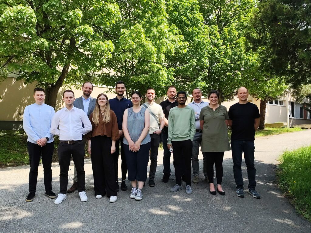
Colleagues from the gallium oxide group led by Dr Filip Gucmann in cooperation with the HUN-REN Centre for Energy Research and Łukasiewicz – Institute of Microelectronics and Photonics have organised two-day workshop on WBG/UWBG #semiconductor materials and devices in Budapest to disseminate the results achieved during the implementation of the CUBES project funded by the…
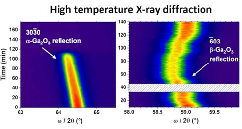
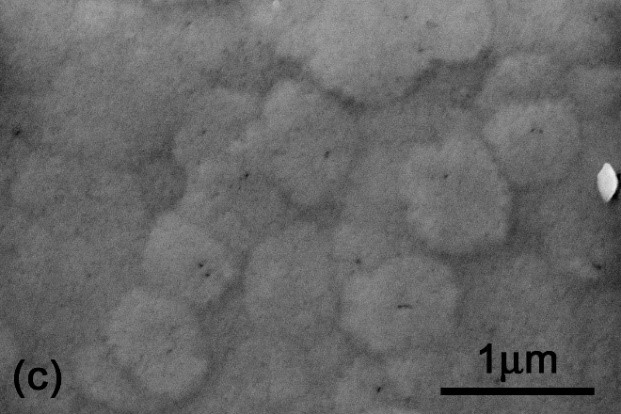
How stable are gallium oxide layers at high temperatures? Scientists from the Institute of Electrical Engineering of the Slovak Academy of Sciences set out to answer this question. Their research provides crucial insights into a promising semiconductor material – gallium oxide (Ga₂O₃) – which has attracted significant interest from both scientific and industrial communities due…
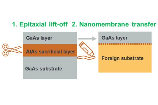
Our colleagues from the department of III-V semiconductors IEE SAS, Slovak University of Technology, and Wuhan University in China have achieved a significant advancement in high-electron-mobility transistor (HEMT) technology prepared from GaAs semiconductor. These devices, crucial for applications in space and defence technologies, high-frequency communication, or quantum computing, where compound-semiconductor amplifiers are widely used. Such…
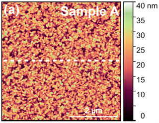
Gallium oxide (Ga2O3) is a promising material for manufacturing of semiconductor devices. The main advantage of Ga2O3 is its large energy gap and the resulting high breakdown field. This allows the use of Ga2O3 epitaxial films for processing of high voltage devices (transistors, diodes), while the wide bandgap opens up the possibilities of its use…
There is a need for novel materials systems that can open a window for sub-THz-frequency electronics. Owing to its record calculated electron velocity, InN is among the hottest candidates. Recent evaluation of the state-of-the art InN grown by molecular-beam-epitaxy (MBE) indicated the electron velocity of about 1 Í 108 cms-1. However, experimental demonstration of InN-channel transistors…