There is a need for novel materials systems that can open a window for sub-THz-frequency electronics. Owing to its record calculated electron velocity, InN is among the hottest candidates.
Recent evaluation of the state-of-the art InN grown by molecular-beam-epitaxy (MBE) indicated the electron velocity of about 1 Í 108 cms-1. However, experimental demonstration of InN-channel transistors is missing to date because of the large lattice misfit between InN and ordinary GaN buffers layers on which InN is normally grown. Elsewhere, it was suggested that InAlN buffer layers with a high In content could resolve this issue by providing better matching.
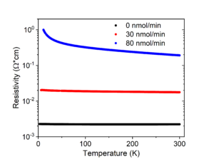
In our work, we studied magnesium-doping of In-rich InAlN layers by using a metal-organic chemical vapor deposition with varied CP2Mg flow between 0 and 130 nmol/min. We concluded that by magnesium-doping of the In-rich InAlN, mobility of free electrons is the main factor which controls the material resistivity. In future, magnesium-doped InAlN material can be tested for the buffer layer in the design of novel InN/InAlN transistor structures.
 Authors: J. Kuzmík, O. Pohorelec, S. Hasenöhrl, M. Blaho, R. Stoklas, E. Dobročka, A. Rosová, Kučera, F. Gucmann, D. Gregušová, M.Precner, A. Vincze, Materials, 16 (2023) 2250
DOI: https://doi.org/10.3390/ma16062250
Prepared by Dr. J. Kuzmik
Authors: J. Kuzmík, O. Pohorelec, S. Hasenöhrl, M. Blaho, R. Stoklas, E. Dobročka, A. Rosová, Kučera, F. Gucmann, D. Gregušová, M.Precner, A. Vincze, Materials, 16 (2023) 2250
DOI: https://doi.org/10.3390/ma16062250
Prepared by Dr. J. Kuzmik
Dependence of the InAlN Hall resistivity on temperature for different Cp2Mg flow.
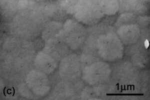
InAlN layer scanning electron microscopy analysis for Cp2Mg flow of 80 nmol/min.