Understanding of the carrier capture-emission processes in the MOS gate structure is necessary to pave the way towards high-effective switching GaN transistors featuring MOS gate structure. Here, we developed a technique capable to separate carrier capture-emission processes by traps located in the oxide bulk and its interface with III-N heterostructure. For the separation, an original technique was used based on the threshold voltage transient monitoring in the MOS-HEMT structure as a function of temperatures and monochromatic light exposure in the energy range of 1.5 to 3.4 eV. We also analyzed in detail the impact of the gate structure properties on its capacitance behavior. Developed technique provides feed-back for technology development of highly-effective switching transistors based on GaN with MOS gate structure. The work was conducted within national APVV project and EU FP7 project HipoSwitch.
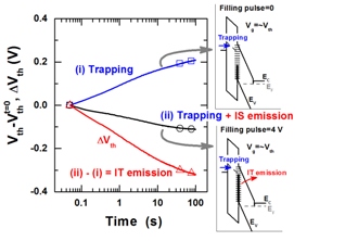
Ťapajna, M., Jurkovič, M., Válik, L., Haščík, Š., Gregušová, D., Brunner, F., Cho, E., and Kuzmík, J.: Bulk and interface trapping in the gate dielectric of GaN based metal–oxide–semiconductor high-electron mobility transistors. Applied Phys. Lett. 102 (2013) 243509.