Nanowires (NW) exhibit unique electrical and optical properties due to lowered dimensions and related confinement effects. An integration of these tiny objects necessitates better understanding of their individual intrinsic properties. Precise electrical characterization of NWs requests preparation of electrical nanocontacts with high stability, low contact resistance and ohmic behaviour. We applied a conventional field-effect transistor configuration that allows to estimate a type of conductivity and carrier mobility also. Structural properties of individual NWs were studied by means of SEM and TEM techniques. The GaP nanowires under study were grown on the p-type GaP (111)B substrate by a VLS technique using 30 nm colloidal gold particles as seeds. A part of NWs was covered by a thin ZnO layer (10 – 140 nm) deposited by RF sputtering. Deposition of thin ZnO layer on the GaP nanowire led to creation of radial PN junction in core-shell configuration. This work was done under support of APVV-0301-10 project.
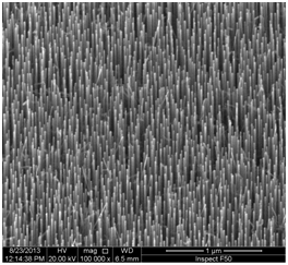
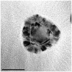
SEM sideview on forrest of GaP nanowires (left) and TEM micrograph (cross-sectional) shows the octahedral structure of a GaP NW core covered with the columnar structure consisted of ZnO grains. The scale bar represents 100 nm (right).
Novák, J., Novotný, I., Kováč, J., Eliáš, P., Hasenöhrl, S., Križanová, Z., Vávra, I., and Stoklas, R.: Preparation of thin Ga-doped ZnO layers for core-shell GaP/ZnO nanowires, Applied Surface Sci 258 (2012) 7607-7611.
Suslik, L., Pudis, D., Skriniarova, J., Kovac, J., Kubicova, I., Tvarozek, P., Martincek, I., and Novak, J.: GaAs/AlGaAs light emitting diode with 2D photonic structure in the surface, Proc. SPIE 8070 (2011) art. no. 807017
Novák, J., Šoltýs, J., Eliáš, P., Hasenöhrl, S., Stoklas, R., Dujavová, A., and Mikulics, M.: Electrical and photoluminescence properties of individual GaP nanowires doped by zinc, Phys. Stat. Solidi (a) 209 (2012) 2505-2512.