Highly Si-doped gallium nitride (n++ GaN) layers play a key role in developing reliable high-electron-mobility transistors (HEMTs) for power and communication electronics.
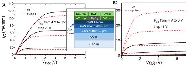
Our researchers from the group of III-V semiconductors investigated their growth using metal-organic chemical vapor deposition (MOCVD) at 800 °C and optimized the silicon precursor flow (SiH₄) to improve both electrical and structural properties. They achieved a free-electron concentration of 7.2 × 10¹⁹ cm⁻³ and mobility of 103 cm²/Vs in an ~8 nm GaN cap layer, which provides effective surface passivation and suppresses the current collapse phenomenon in HEMTs.
“As we have shown, the free electrons in the n++ GaN cap efficiently screen the surface potential, keeping the transistor channel stable and ensuring collapse-free operation,” explains Dr. Ján Kuzmík, the first author of the study.
The team further demonstrated that flow-modulation epitaxy can increase the maximum carrier concentration up to 10²⁰ cm⁻³, offering new design freedom for normally-off GaN/InAlN/AlN HEMTs. These findings underline the importance of precisely controlled doping and low-temperature growth for next-generation GaN devices.
The results were published in Materials Science in Semiconductor Processing.

Output characteristics of HEMTs with a) 8 nm and b) 6 nm n++ cap (dark green) in dc and pulsed regime.


