






Researchers from the Institute of Electrical Engineering of the SAS, in collaboration with the Institute of Physics SAS, the Centre for Advanced Materials Applications (CEMEA), and the Elettra synchrotron facility in Trieste, have clarified how ultrathin platinum diselenide (PtSe2) films form during thermal conversion. Real-time in-situ X-ray scattering made it possible to directly follow the crystallisation process and determine key parameters governing material growth.
Two-dimensional materials are promising building blocks for future electronics, optoelectronics, and sensing technologies. Their properties can change substantially when their thickness is altered by only a few atomic layers. One such material is platinum diselenide, PtSe2, which can behave as a semiconductor when ultrathin and as a semimetal in thicker films.
For practical applications, it is essential to produce high-quality, uniform PtSe2 films over larger areas and to understand the processes that take place during their growth. The research team therefore investigated PtSe2 formation directly during thermally assisted conversion in selenium vapor. In this process, a pre-deposited platinum layer is transformed into layered PtSe2 while being heated.
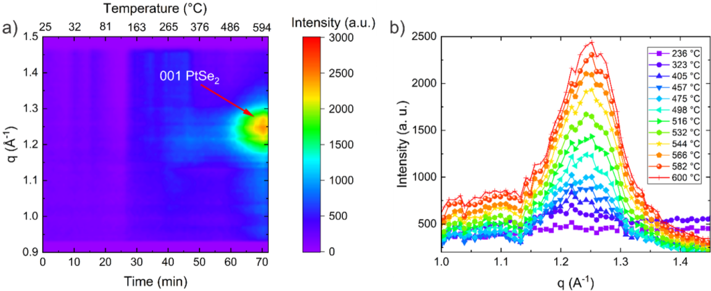
The transformation was monitored in real time using grazing-incidence wide-angle X-ray scattering, known as GIWAXS. The experiment was performed at the Elettra synchrotron facility in Trieste, Italy, allowing the researchers to observe the emergence and structural evolution of the crystalline PtSe2 phase during growth.
The measurements showed that crystalline PtSe2 begins to form at approximately 400 °C. The material grew with its layers aligned parallel to the substrate surface, and no detectable metastable intermediate phases were observed during the selenization process.
The researchers applied the Avrami model to describe the crystallisation kinetics. This analysis yielded an effective activation energy for PtSe2 crystallisation of 93 ± 11 kJ/mol, representing the dominant energy barrier associated with formation of the crystalline phase during thermally assisted conversion.
The measurements also revealed that structural evolution continues after the crystalline PtSe2 phase has formed. As the temperature increases, the spacing between adjacent PtSe2 layers contracts, while other lattice parameters evolve. These changes are associated with strain relaxation, improved crystallinity, and gradual structural adjustment of the film to the substrate.
The study provides a more detailed understanding of PtSe2 growth by thermally assisted conversion. Combining real-time structural monitoring with kinetic modelling can help optimise the preparation of PtSe2 and other two-dimensional materials, supporting their eventual integration into electronic, optoelectronic, and sensing devices.
Authors: Jana Hrdá, Karol Vegso, Ashin Shaji, Peter Nádaždy, Timea Ema Krajčovičová, Lenka Pribusová Slušná, Sigrid Bernstorff, Matej Jergel, Peter Siffalovic, Martin Hulman
Link: https://iopscience.iop.org/article/10.1088/2632-959X/ae72aa