Gallium nitride (GaN)-based semiconductors are increasingly used for the fabrication of highly efficient power converters. Our colleagues have succeeded in confirming the functionality of an original concept for a vertical power transistor.
Modern GaN power transistors with lateral channel geometry are gradually commercialized and used in electronic industry. Compared to this concept, the vertical geometry is useful for increasing the device performance and suppressing parasitic effects such as self-heating and output current instability. However, the preparation of vertical structures is quite complex as it involves problematic hole-doping for GaN or nano-patterning by electron beam lithography. Our colleague Jan Kuzmik has recently designed and patented a simplified preparation of a vertical transistor using a carbon-doped semi-insulated GaN channel. In the current work, we demonstrate for the first time the functionality of this new concept. Robust component design without the need for hole doping, good breakdown voltage scalability without reducing the electron doping of the drift region, and high electron mobility in the channel represent the main benefits of this concept. Therefore, our study pawe the way for further development of these devices.
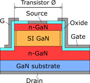
Schematic cross-section of the GaN vertical transistor structure.
Šichman, P., Stoklas, R., Hasenöhrl, S., Gregušová, D., Ťapajna, M., Hudec, B., Haščík, Š., Hashizume, T., Chvála, A., Šatka, A., and Kuzmík, J.: Vertical GaN transistor with semi-insulating channel, Physica Status Solidi (a) 220 (2023) SI2200776.