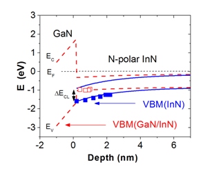
InN is material with the highest saturated velocity of electrons from all existing semiconductors. Consequently, InN is a candidate for designing extremely fast transistors. However, till now there is no report on InN-based microwave transistors. This is because of high strain from the back-side if InN is grown on GaN and because of electron accumulation on the InN surface. In our work we analyzed electrical and chemical properties of InN layers grown with different polarity and methods of removing electrons surface accumulation. Significant oxidation at the In-polar InN surface was found by analyzing photo-electrons emitted from atoms core shells. Similarly, we observed significant surface electron accumulation regardless of the oxide presence. On the other hand, if the InN was capped by four mono-layer of GaN, surface accumulation was fully removed. This effect is vital for manufacturing future ultra-fast InN transistors.
Kuzmik, J., Haščík, Š., Kučera, M., Kúdela, R., Dobročka, E., Adikimenakis, A., Mičušík, M., Gregor, M., Pleceník, A., and Georgakilas, A.: Elimination of surface band bending on N-polar InN with thin GaN capping, Applied Phys. Lett. 107 (2015) 191605.
Kuzmík, J., Adikimenakis, A., Gregor, M., Mičušík, M., Eičo, K., Haščík, Š., Plecenik, A., and Georgakilas, A.: Impact of polarity and GaN capping on electrical and material properties of InN surfaces. In: 11th Inter. Conf. on Nitride Semicond. Peking, 2015.