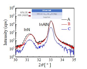
InN has been recognized as a far-reaching candidate for ultra-high-speed electronics since almost two decades ago. Indeed, very recently these expectations were supported by us extracting the electron drift velocity of 1 ×108 cm/s in 775-nm thick InN, the highest ever reported value in any semiconductor material. We report proof-of-concept N-polar InN/In0.61Al0.39N heterostructures. 20-nm thick InN has been MOCVD grown on Mg-doped InAlN buffer with an optional AlN spike as an interlayer between the InAlN buffer and the InN channel, or as a part of InAlN nucleation on sapphire. Our findings prove potential of InN for a future generation of fast electronics. If the technology is fully developed, present THz frequency gap between the electronic and optical devices will be erased.
Kuzmík, J., Stoklas, R., Hasenöhrl, S., Dobročka, E., Kučera, M., Eliáš, P., Gucmann, F., Gregušová, D., Haščík, Š., Kaleta, A., Chauvat, M.P., Kret, S., and Ruterana, P.: InN/InAlN heterostructures for new generation of fast electronics, J. Applied Phys. 135 (2024) 245701.