Gallium oxide (Ga2O3) is a modern, ultra-wide bandgap semiconductor material with a bandgap energy of up to 4.9 – 5.3 eV and, compared to conventional semiconductors, possesses a significantly larger critical breakdown field (>8 MV/cm). This makes it suitable for the fabrication of microelectronic structures and devices that require handling high voltages and power levels. Ga2O3 a IVth generation semiconductor that fundamentally expands the capabilities previously offered by semiconductors such as GaN and SiC, as well as III-V materials before them. Ga2O3-based devices are particularly applicable in electric energy conversion systems, such as switching power supplies in consumer electronics and electromobility, high-voltage rectifiers, and in the detection of deep UV radiation for fire prevention and in the defense sector.
We engage in fundamental material research on the epitaxial growth of Ga2O3 layers using metal-organic chemical vapour deposition (MOCVD) techniques on foreign substrates to improve the heat dissipation caused by self-heating in Ga2O3 devices, as well as to prepare cost-effective, large-area layers that would facilitate the broader adoption of Ga2O3 technology in industry.
We are also involved in the development and fabrication of Ga2O3-based microelectronic devices —primarily switching metal-oxide-semiconductor field-effect transistors (MOSFET), rectifying diodes, and photodetectors for the deep UV range based on metal-semiconductor-metal (MSM) structures, or heterostructures in combination with synthetic diamond, NiO, etc.
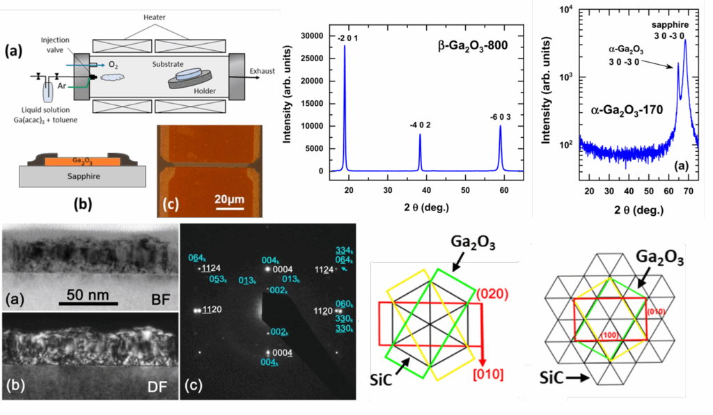
We have successfully achieved the epitaxial growth of various Ga2O3 phases (α, β, κ) on sapphire and SiC substrates using MOCVD.
We significantly contribute to the understanding and mitigation of limitations related to self-heating in Ga2O3-based devices. We predicted that Ga2O3 MOSFETs fabricated on SiC substrates using our technology could lead to a substantial reduction in their operating temperature—up to nearly 300 times lower compared to those on Ga2O3 substrates.
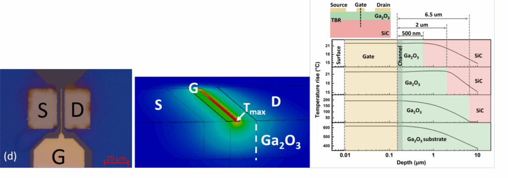
Additionally, we have expanded knowledge regarding the thermal properties of very thin Ga2O3 layers of various phases and the thermal boundary conductance (TBC) at the interface between the Ga2O3 layer and the foreign substrate.

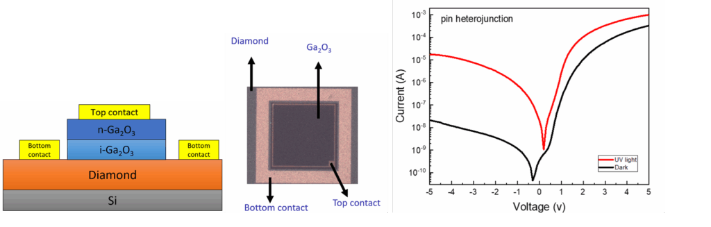
We have developed and fabricated heterostructure photodiodes combining n-type Ga2O3 and p-type diamond, which are insensitive to visible light while being highly sensitive in the UV range—suitable, for e.g., for flame detection, corona discharge in high-voltage power distribution lines, or in the defense and space industries.
Publications:
Xiao, X., Mao, Y., Meng, B., Ma, G., Hušeková, K., Egyenes, F., Rosová, A., Dobročka, E., Eliáš, P., Ťapajna, M., Gucmann, F., and Yuan, C.: Phase-dependent phonon heat transport in nanoscale gallium oxide thin films, Small 20 (2024) 2309961.
Gucmann, F., Nádaždy, P., Hušeková, K., Dobročka, E., Priesol, J., Egyenes, F., Šatka, A., Rosová, A., and Ťapajna, M.: Thermal stability of rhombohedral α- and monoclinic β-Ga2O3 grown on sapphire by liquid-injection MOCVD, Mater. Sci Semicond. Process. 156 (2023) 107289.
Hrubišák, F., Hušeková, K., Zheng, X., Rosová, A., Dobročka, E., Ťapajna, M., Mičušík, M., Nádaždy, P., Egyenes, F., Keshtkar, J., Kováčová, E., Pomeroy, J.W., Kuball, M., and Gucmann, F.: Heteroepitaxial growth of Ga2O3 on 4H-SiC by liquid-injection MOCVD for improved thermal management of Ga2O3 power devices, J. Vacuum Sci Technol. A 41 (2023) 042708.
Dobročka, E., Gucmann, F., Hušeková, K., Nádaždy, P., Hrubišák, F., Egyenes, F., Rosová, A., Mikolášek, M., and Ťapajna, M.: Structure and thermal stability of ε/κ-Ga2O3 films deposited by liquid-injection MOCVD, Materials 16 (2023) 20.
Egyenes, F., Gucmann, F., Rosová, A., Dobročka, E., Hušeková, K., Hrubišák, F., Keshtkar, J., and Ťapajna, M.: Conductance anisotropy of MOCVD-grown α-Ga2O3 films caused by (010) β-Ga2O3 filament-shaped inclusions, J. Phys. D: Appl Phys. 56 (2023) 045102.
Ťapajna, M., Egyenes, F., Hrubišák, F., Hušeková, K., Dobročka, E., Nádaždy, P., Rosová, A., Chouhan, H., Keshtkar, J., and Gucmann, F.: Liquid-injection MOCVD-grown Ga2O3 on sapphire and 4H-SiC substrates: Material, transport, and MOSFET properties. In: IMFEDK 2023: Inter. Meeting for Future of Electron Devices, Kansai. – IEEE, 2023, p. IN10. ISBN 979-8-3503-9378-1.
Hrubišák, F., Hušeková, K., Egyenes, F., Rosová, A., Kubranská, A., Dobročka, E., Nádaždy, P., Keshtar, J., Gucmann, F., and Ťapajna, M.: Structural and electrical properties of Ga2O3 transistors grown on 4H-SiC substrates. In: ASDAM 2022. Eds. J. Marek et al. IEEE 2022. ISBN 978-1-6654-6977-7. P. 115-118.
Egyenes, F., Gucmann, F., Dobročka, E., Mikolášek, M., Hušeková, K., and Ťapajna, M.: Transport properties of Si-doped ẞ-Ga2O3 grown by liquid-injection MOCVD. In: ASDAM 2022. Eds. J. Marek et al. IEEE 2022. ISBN 978-1-6654-6977-7. P. 119-122.
Egyenes-Pörsök, E., Gucmann, F., Hušeková, K., Dobročka, E., Sobota, M., Mikolášek, M., Fröhlich, K., and Ťapajna, M.: Growth of α- and β-Ga2O3 epitaxial layers on sapphire substrates using liquid-injection MOCVD, Semicond. Sci Technol. 35 (2020) 115002.